

Page 1
HF/VHF/UHF N-CHANNELMOSFETs
■ GOLDMETALLIZATION
■ EXCELLENTTHERMALSTABILITY
■ COMMONSOURCE CONFIGURATION
■ POUT = 150W MIN. WITH 12.5 dB gain @175
MHz
DESCRIPTION
The SD2921is a gold metallizedN-ChannelMOS
field-effect RF power transistor. The SD2921 is
intended for use in 50V dc large signal
applicationsup to 200 MHz
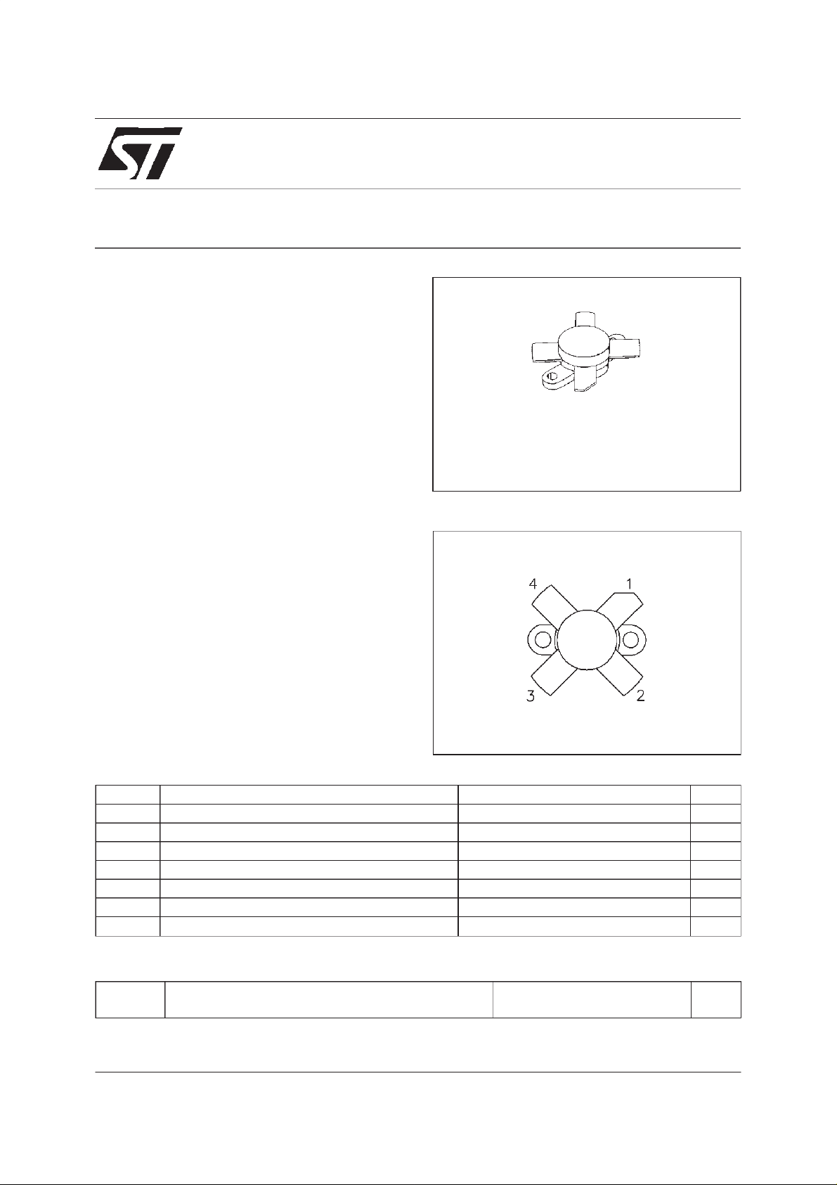
SD2921
RF POWER TRANSISTORS
M174
epoxy sealed
ORDER CODE BRANDING
SD2921 SD2921
PIN CONNECTION
1. Drain 3.Gate
2. Source 4. Source
ABSOLUTE MAXIMUM RATINGS (T
Symb o l Parameter Val u e Uni t
V
(BR)DSS
V
V
P
T
Drain So urc e Volt age 125 V
Drain-G at e Voltage (RGS=1MΩ) 125 V
DGR
Gat e- Source V olt age ±20 V
GS
Drain Cur re nt 16 A
I
D
Power Diss ipation 292 W
DISS
Max. Oper ating J unct ion T emperatu re 200
T
j
Storage T emperature -65 to 150
STG
case
=25oC)
THERMAL DATA
R
th(j-c)
R
th(c-s)
* Determined using a flat aluminum or copperheatsink with thermal compound applied (Dow Corning340 or equivalent).
November 1999
Junct ion- Ca se Therm al Resist anc e
Case-Heat s i nk Therm al R esis tance ∗
0.6
0.2
o
o
o
C/W
o
C/W
C
C
1/10
Page 2
SD2921
ELECTRICAL SPECIFICATION (T
case
=25oC)
STATIC
Symb o l Para met er Mi n . Typ . Max. Unit
V
(BR)DSSVGS
I
DSS
I
GSS
V
GS(Q)
V
DS(ON)VGS
G
FS
C
ISS
C
OSS
C
RSS
=0V IDS= 100 m A 125 V
VGS=0V VDS=50V 5 mA
VGS= 20V VDS=0V 5 µA
VDS= 10V ID= 250 m A 1.0 5.0 V
= 10V ID=10A 3.0 V
VDS= 10V ID=5A 4 mho
VGS=0V VDS= 50 V f = 1 M H z 411 pF
VGS=0V VDS= 50 V f = 1 M H z 198 pF
VGS=0V VDS=50V f=1MHz 27 pF
DYNAMIC
Symb o l Para met er Mi n . Typ . Max. Unit
P
OUT
G
η
Load
Mismatch
f = 175 M H z VDD=50V IDQ= 250 mA 150 W
f = 175 M H z VDD=50V P
PS
f = 175 M H z VDD=50V P
D
f = 175 M H z V
DD
=50V P
=150W IDQ= 250 m A 12.5 14 dB
out
=150W IDQ= 250 mA 55 65 %
out
=150W IDQ=250mA
out
10:1 VSWR
All Phase Angles
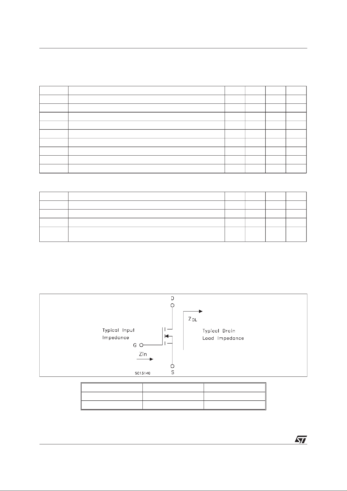
REF. 1021304K
IMPEDANCEDATA
2/10
FREQ. ZIN(Ω)Z
DL
(Ω)
30 M Hz 1. 7 - j 5.7 6.8 + j 0.9
175MHz 1.2-j2.0 2.0+j2.4
Page 3
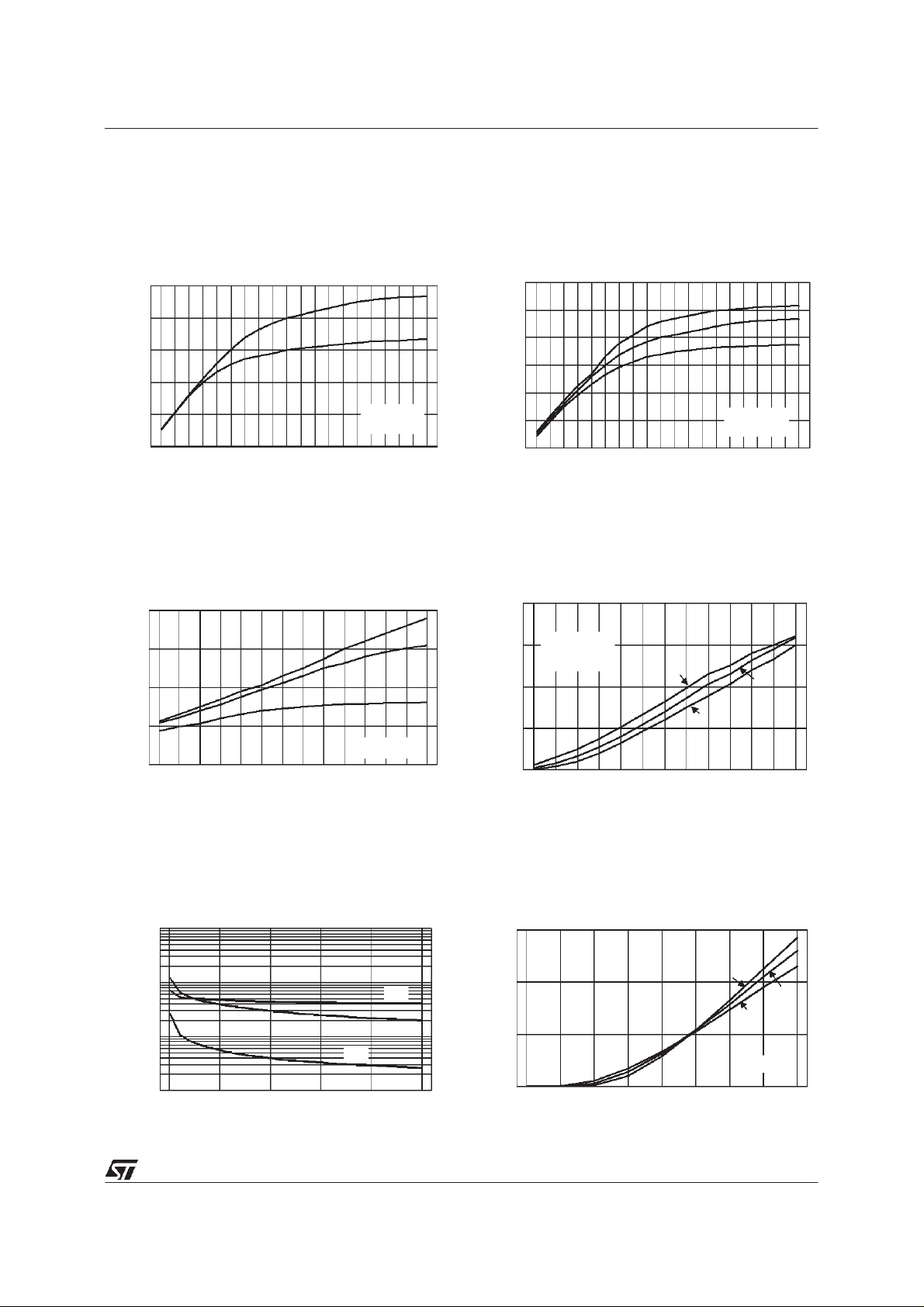
TYPICALPERFORMANCE
SD2921
OutputPowervs Input Power
250
200
150
100
50
Pout, OUTPUT POWER (W)
0
14710131619
Pin, INPUT POWER (W)
Vdd = 50V
OutputPowervs SupplyVoltage
200
150
100
50
Pout, OUTPUT POWER (WATTS)
0
24 28 32 36 40 44 48
VDD, SUPPLY VOLTAGE (VOLTS)
Pin = 9W
Vdd =40V
Tc = 25°C
f =175 MHz
IDQ = 250mA
Pin = 6W
Pin = 3W
IDQ = 250mA
f =175MHz
OutputPower vs Input Power
300
250
200
150
100
50
Pout, OUTPUT POWER (W)
0
1 3 5 7 9 1113151719
Pin, INPUT POWER (W)
OutputPower vs GateVoltage
200
VDD = 50V
150
IDQ = 250mA
f = 175MHz
Pin = Constant
100
50
Pout, OUTPUT POWER (W)
0
-3 -2 -1 0 1 2 3
VGS, GATE-SOURCE VOLTAGE (VOLTS)
T = -20°C
Tcase =-20°C
Tcase = 25°C
Tcase = 80°C
IDQ = 250 mA
VDD = 50V
f =175MHz
T=80°C
T=25°C
Capacitancevs Drain-SourceVoltage
10000
1000
100
C, CAPACITANCE(pF)
10
0 1020304050
VDS,DRAIN-SOURCEVOLTAGE(VOLTS)
Crss
Ciss
Coss
Drain Current vs Gate Voltage
15
10
5
ID, DRAIN CURRENT (A)
0
2 2.5 3 3.5 4 4.5 5 5.5 6
VGS,GATE-SOURCEVOLTAGE(VOLTS )
T = -20°C
T=25°C
T=80°C
VDS= 10V
3/10
Page 4

SD2921
TYPICALPERFORMANCE
Gate-SourceVoltagesvs Case Temperature
OutputPower vs GateVoltage
200
1.1
1.05
1
0.95
0.9
0.85
VGS, GATE-SOURCE VOLTAGE (NORMALIZED
-25 0 25 50 75 100
VDS = 10V
Tc, CASE TEMPERATURE (°C)
Id = 5A
Id = 4A
Id = .25A
Id = .1A
Id = 2A
Id = 1A
150
VDD= 50 V
IDQ= 250 mA
f = 30MHz
100
Pout, OUTPUT POWER(W)
FixedPin
50
0
012345 6
VGSGATE-SOURCE VOLTAGE (V)
PowerGainvs Output Power OutputPower vs Input Power
26.5
26
25.5
PG, POWER GAIN(dB)
25
24.5
f =30MHz
VDD= 50 V
IDQ= 250mA
0 50 100 150 200
Pout, OUTPUT POWER (W)
SC13170
250
200
150
100
50
Pout, OUTPUT POWER(W)
0
0.02 0.1 0.18 0.26 0.34 0.42 0.5 0.58 0.66
Pin, INPUT POWER (W)
Tfl= 25°C
VDD= 50 V
Tfl= -20°C
Tfl= 80°C
VDD= 40 V
f=30MHz
IDQ= 250mA
SC13 210
SC13180
Efficiency vs Output Power
60
40
Efficiency(%)
20
0
0 50 100 150 200
Pout,OUTPUTPOWER(W)
4/10
f= 30M Hz
VDD= 50 V
IDQ= 250mA
SC13190
OutputPower vs VoltageSupply
200
150
100
50
Pout, OUTPUT POWER (W)
0
24 28 32 36 40 44 48
VDD,SUPPLY VOLTAGE (V)
Pin= 0.6W
f= 30 MHz
IDQ= 250 mA
Pin= 0.4W
Pin= 0.2W
SC132 00
Page 5

SD2921
MaximumThermalResistancevsCase
Temperature
0.75
0.7
0.65
RTH(j-c) (ºC/W)
0.6
0.55
25 45 65 85
Tc, CASE TEMPERATURE (ºC)
DC Safe OperatingArea
100
50
30
20
(1)
10
Ids(A)
5
3
2
1
1 2 5 10 20 50 100 200
(1) Currentin this area may be limited by Rds(on)
Vds(V)
5/10
Page 6

SD2921
30 MHzTestCircuit Schematic (EngineeringTest Circuit)
V +G
30 MHzTestCircuit Component Part List
+50V
T1 9:1 Transformer, 25 ohm Flexible Coax with extra shield.090 OD 15” Long
T2 1:4 Transformer, 50 ohm Flexible Coax .225 OD 15” Long
FB1 Toroid, 1.7” OD.30” ID 220u4 Turns
FB2 SurfaceMount EMI Shield Bead
FB3 Toroid, 1.7” OD.300” ID 220u3 Turns
RFC1 Toroid, 0.5” OD 0.30” ID, 125u4 turns 12 awg wire
PCB 0.062” WovenFiberglass, 1 oz. Copper,2 Sides, er= 2.55
C1, C4, C6, C7, C8, 0.01uF ATCChip Cap C5 470pF ATCChip Cap
C9, C11, C12, C13 0.01 uF ATCChip Cap C10 10 uF 63V Electrolytic Capacitor
C2, C3 750 pF ATCChipCap C14 100 uF 63V Electrolytic Capacitor
R1, R3 1K ohm 1W Chip Resistor R2 680ohm 3W WirewoundResistor
6/10
Page 7

175 MHz Test Circuit Schematic (ProductionTestCircuit)
V
G +50V
SD2921
Note : All dimensions in inches
REF. 1021579C
175 MHz Test Circuit Component Part List
T1 4:1 Transformer, 25 ohm Flexible Coax .090 OD 6 ” Long
T2 1:4 Transformer, 25 ohm Semi-RigidCoax .141 OD 6 ” Long
FB1 Toroid X2, 0.5” OD .312” ID 850u 2 Turns
FB2, FB3 VK200
FB4 Shield Bead, 1” OD 0.5” ID 850u 3 Turns
L1 1/4Wave Choke, 50 ohm Semi-Rigid Coax .141 OD 12 ” Long
PCB 0.062” Woven Fiberglass, 1 oz. Copper, 2 Sides, er = 2.55
R1, R3 470 ohm 1W Chip Resistor R4 20K ohm 10 Turn Potentiometer
R2 360 ohm 1/2W Resistor R5 560 ohm 1W Resistor
C1, C11 470 pF ATCChip Cap C7 30 pF ATCChip Cap
C2 43 pF ATC Chip Cap C10 91 pF ATC Chip Cap
C3, C8, C9 Arco 404, 12-65 pF C12, C15 1200 pF ATC Chip Cap
C4 Arco 423, 16-100 pF C13, C14 0.01 uF / 500V Chip Cap
C5 120 pF ATCChip Cap C16, C17 0.01 uF / 500V Chip Cap
C6 0.01 uF ATCChip Cap C18 10 uF 63V Electrolytic Capacitor
7/10
Page 8

SD2921
175 MHz Test Circuit Photomaster
175 MHz Test Circuit
8/10
Page 9

M174 (.500 DIA 4L N/HERM W/FLG) MECHANICALDATA
SD2921
DIM.
MIN. TYP. MAX. MIN. TYP. MAX.
A 5.56 5.84 0.219 0.230
B 3.18 0.125
C 6.22 6.48 0.245 0.255
D 18.28 18.54 0.720 0.730
E 3.18 0.125
F 24.64 24.89 0.970 0.980
G 12.57 12.83 0.495 0.505
H 0.08 0.18 0.003 0.007
I 2.11 3.00 0.083 0.118
J 3.81 4.45 0.150 0.175
K 7.11 0.280
L 25.53 26.67 1.005 1.050
M 3.05 3.30 0.120 0.130
mm inch
Controlling Dimension in Inches
1011000D
9/10
Page 10

SD2921
Information furnished isbelieved tobe accurate and reliable. However, STMicroelectronics assumes no responsibility for theconsequences
of use of such information nor for any infringement of patents or other rights of third parties which may result from its use. No license is
granted by implication or otherwise under any patent or patent rights of STMicroelectronics. Specification mentioned in this publication are
subject to change without notice. This publication supersedes andreplaces allinformation previously supplied. STMicroelectronics products
are not authorized for use as critical components in life support devices or systems without express written approval of STMicroelectronics.
The ST logo is a trademark of STMicroelectronics
1999 STMicroelectronics – Printed in Italy – All Rights Reserved
STMicroelectronicsGROUP OF COMPANIES
Australia - Brazil - China - Finland - France - Germany- Hong Kong - India - Italy- Japan - Malaysia - Malta - Morocco -
Singapore- Spain - Sweden - Switzerland -United Kingdom -U.S.A.
http://www.st.com
.
10/10
 Loading...