

SATELLITE COMM UNIC ATIONS APPLICATI ONS
REFRACTORY/GOLD METALLIZATION
.
EFFICIENCY - 50% TYPICAL
.
.
P
OUT =
30 W MIN. WITH 9.3 dB GAIN
SD1899
RF & MICR OWAVE TRANSIST ORS
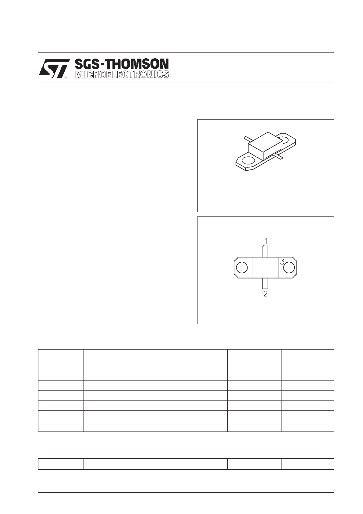
.250x.3202LFL(M170)
epoxy sealed
ORDER CODE
SD1899
PIN CONNE CT I O N
BRANDING
SD1899
DESCRIPTION
The SD1899 is a commonbasesiliconNPNbipolar
device optimized for 1.6 GHz SATCOM applications.
SD1899 offers superior gain and collector efficiency, making it an idealchoice for ClassC power
amplifiers used in portable as well as fixed SATCOM terminals.
ABSOL UTE MAXIMUM RATINGS (T
Symbol Parameter Valu e Unit
V
V
V
P
T
CBO
CES
EBO
I
C
DISS
T
J
STG
Collector-Base Voltage 45 V
Collector-EmitterVoltage 45 V
Emitter-Base Voltage 3.0 V
Device Current 3.5 A
Power Dissipation (+25°C) 64.8 W
Junction Temperature +200
Storage Temperature
case
= 25°C)
1. Collector 3. Base
2. Emitter
65 to +150
−
°
C
°
C
THERMAL DATA
R
TH(j-c)
January 6, 1997 1/5
Junction-CaseThermal Resistance 2.7 °
C/W

SD 1899
ELECTRICAL SPECIFICATI ONS
(T
case
25°C)
=
STATIC
Symbol Test Conditions
BV
CBO IC = 8 mA IE = 0 mA
BV
CES IC = 8 mA VBE = 0 V
BV
EBO IE = 8 mA IC = 0 mA
I
CBO VCB = 28 V IE = 0 mA
h
FE VCE = 5 V IC = 1.6 A
DYNAMIC
Symbol Test Conditions
P
OUT
η
P
f = 1650 MHz VCC = 28 V PIN = 3.5 W
c f = 1650 MHz VCC = 28 V PIN = 3.5 W
f = 1650 MHz VCC = 28 V
G
Value
Min. Typ. Max.
Unit
45 — — V
45 — — V
3.0 — — V
——2mA
15 — 150 —
Value
Min. Typ. Max.
Unit
30 32 — W
45 50 — %
9.3 — — dB
2/5 January 6, 1997

TYPIC AL PERFORMANCE
POWER INPUT vs POWER OUTPUT POWER INPUT vs EFFICIENCY
SD 1899
POWER INPUT vs POWER OUTPUT
POWER INPUT vs POWER OUTPUT
POWER INPUT vs EFFICIENCY
POWER INPUT vs EFFICIENCY
January 6, 1997 3/5

SD 1899
TEST CIRCUI T
C1: .3 - 1.2 pf Johanson Capacitor
C2: .4 - 2.5 pf Johanson Capacitor #27283
C3: 100 pf Chip Capacitor ATC 100 A101KCA 150
C4: 15,000 pf EMI filter Murata/Erie 9900-381-6604
L1, L2 :4 Turn Choke #28 AWG .080”I.D.
Board Material:
EPSILAM 10, Er
1Oz. Copper, SMA Launcher CDI (2 pieces)
= 10.2, .050” Thick,
4/5 January 6, 1997

PACKAG E MECHANI CAL DATA
Ref.: Dwg. No.:12-0170
UDCS No. 1010996 rev. B
SD 1899
Information furnished is believed to be accurate and reliable. However, SGS-THOMSON Microelectronics assumes no responsibility for the
consequences of use of such information nor for any infringement of patents or other rights of third parties which may result from its use.
No license is granted by implication or otherwise under any patent or patent rights of SGS-THOMSON Microelectronics. Specifications
mentioned in this publication are subject to change without notice. This publication supersedes and replaces all information previously
supplied. SGS-THOMSON Microelectronics products are not authorized for use as critical components in life support devices or systems
without express written approval of SGS-THOMSON Microelectronics.
1997 SGS-THOMSON Microelectronics - All Rights Reserved
Australia - Brazil - Canada - China - France - Germany - Italy - Japan - Korea
Malaysia - Malta - Morocco - The Netherlands - Singapore - Spain - Sweden - Switzerland
SGS-THOMSON Microelectronics GROUP OF COMPANIES
Taiwan - Thailand - United Kingdom - U.S.A.
January 6, 1997 5/5
 Loading...