

RF & MICROWAVE TRANSISTORS
.DESIGNED FOR HIGH PO WER PULSED
IFF APPLICATIONS
.450 WATTS (min.) IFF 1030/1090 M Hz
. 7.0 dB MIN. GAIN
.REFRACTORY GOLD METALLIZATION
.BALLASTING AND LOW THERMAL
RESISTANCE FOR RELIABILIT Y AND
RUGGEDNESS
.30:1 LOAD VSWR CAPABILITY AT
SPECIFIED OPERATING C ON D ITION S
. INPUT MATCHED , C OMMON BASE
CONFIGURATION
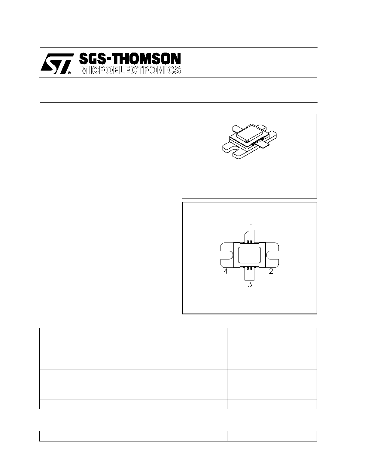
SD1541-09
AVIONI CS APPLICA TIONS
.400 x .500 2LF L (M112)
hermetically sealed
ORDER CODE
SD1541-09
PIN CONNECTION
BRANDING
1541-9
DESC RIPT ION
The SD1541-09 is a gold metallized silicon NPN
planar transistor. The SD1541-09 is designedfor
applications requiring high peak and low duty cycles such as IFF. The SD1541-09 is packaged in
a metal/ceramic package with internal input matching, resulting in improved broadband performance
and a low thermal resistance.
ABSOLUTE MAXIMUM RATINGS (T
Symbol Parameter Value Uni t
V
CBO
V
CEO
V
EBO
I
C
P
DISS
T
J
T
STG
THERMA L DA TA
R
TH(j-c)
Collector-Base Voltage 65 V
Collector-Emitter Voltage 65 V
Emitter-Base Voltage 3.5 V
Device Current 22 A
Power Dissipation 1458 W
Junction Temperature +200
Storage Temperature
Junction-Case Thermal Resistance 0.12 °C/W
case
= 25°C)
1. Collector 3. Emitter
2. Base 4. Base
65 to +150
−
°
C
°
C
November 1992
1/4
SD1541-09
ELECTRICAL SPECIFICA TIONS (T
case
= 25°C)
STATIC
Symbol Test Conditions
BV
BV
BV
I
CES
h
CBO
CES
EBO
FE
IC= 25mA IE= 0mA 65 — — V
IC= 50mA IB= 0mA 65 — — V
IE= 10mA IC= 0mA 3.5 — — V
VCE= 50V IE= 0mA — — 25 mA
VCE= 5V IC= .25A 5 — 200 —
DYNAMIC
Symbol Test Cond iti ons
P
OUT
G
P
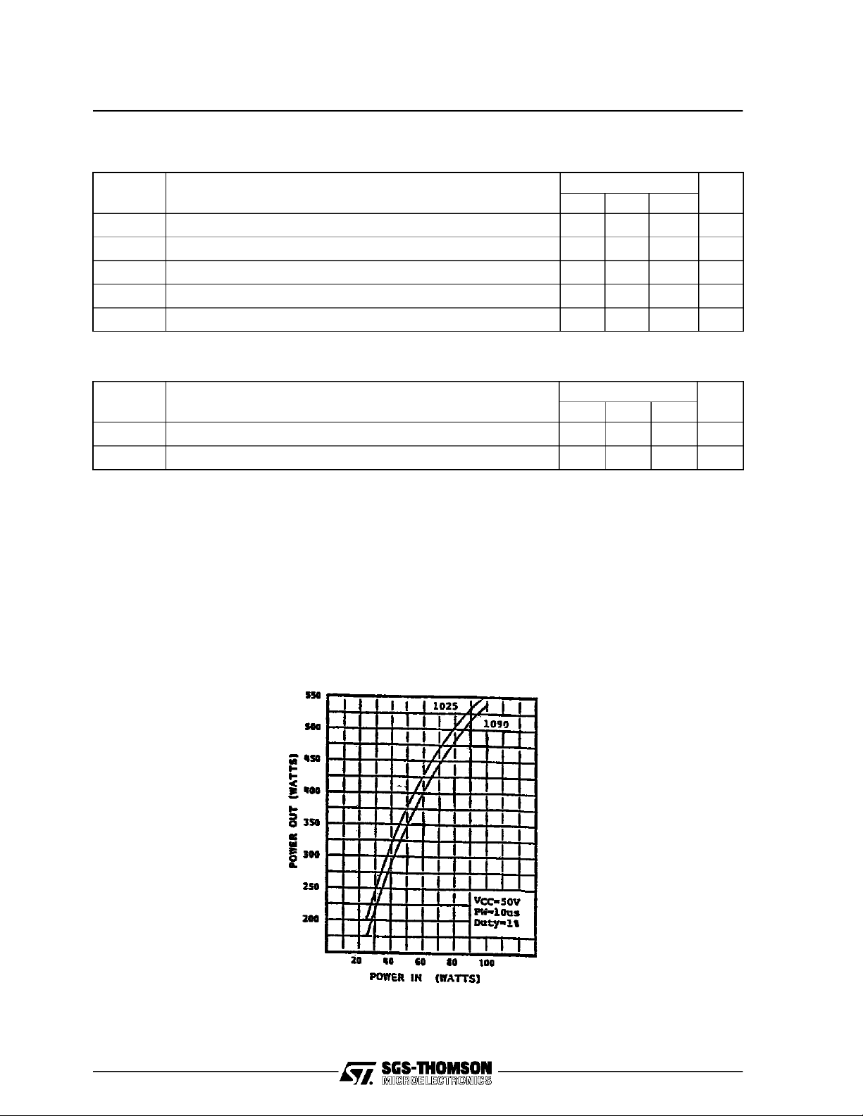
Note: Pulse Width= 10µSec, Duty Cycle= 1%
f = 1090 MHz PIN= 90 W VCE= 50 V 450 — — W
f = 1090 MHz PIN= 90 W VCE= 50 V 7.0 — — dB
Value
Min. Typ. Max.
Value
Min. Typ. Max.
Unit
Unit
TYPICA L PERFO R MA NCE
POWER OUTPUT vs POWER INPUT
2/4

IMPEDA NCE DATA
TYPICAL INPU T
IMPEDANCE
Z
IN
TYPICAL COLLECTOR
LOAD IMPEDANCE
Z
CL
TEST CIRC UIT L AYO UT
FREQ. ZIN(Ω)Z
CL
(Ω)
1030 MHz 1.6 + j 5.1 1.1 − j2.0
1090 MHz 2.5 + j 4.7 1.2 − j1.2
SD 1541-09
C1 : .4 - 2.5pF Johanson Gigatrim
C2 : 100pF Chip Capacitor
C3 : .01µfD CK05BX103K
C4 : 1000µfD Electrolytic 63V
C5 : 100pF Chip Capacitor
L1 : 1/2 Turn .026” Diameter Wire
Loop=.170” Width x .320” Height
L2 : 1 Turn .026” Diameter Wire I.D. .130”
All Dimensions are in Inches
Board Er=10.2, Height .025”
3/4

SD1541-09
PACKAGE MECHANICAL DATA
Ref.: Dwg. No.12-0112
Information furnished isbelieved to be accurate and reliable.However, SGS-THOMSON Microelectronics assumesno responsability for the
consequences of useof such information nor for any infringementof patents or other rights of third parties which may results from its use. No
license is granted by implication or otherwise under any patentor patent rights of SGS-THOMSON Microelectronics. Specificationsmentioned
in this publication are subject to change without notice. This publication supersedes and replaces all information previously supplied.
SGS-THOMSON Microelectronicsproductsare notauthorized foruse ascritical componentsin life supportdevices orsystems without express
written approval of SGS-THOMSON Microelectonics.
1994 SGS-THOMSON Microelectronics- All Rights Reserved
Australia - Brazil - France - Germany - Hong Kong - Italy - Japan - Korea - Malaysia - Malta - Morocco - The Netherlands -
Singapore -Spain - Sweden - Switzerland - Taiwan - Thailand - United Kingdom - U.S.A
SGS-THOMSON Microelectronics GROUP OF COMPANIES
4/4
 Loading...