


.860 MHz
.20 VOLTS
.COMMON EMITTER
.GOLD METALLIZATION
.CLASS A LINEAR OPERATION
.P
= 1.0 W MIN. WITH 10.0 dB GAIN
OUT
SD1449 (TCC597)
RF & MICROWAVE TRANSISTORS
UHF TV\LINEAR APPLICATIONS
.280 4L STUD (M122)
epoxy sealed
ORDER CO DE
SD1449
PIN CONNECTION
BRANDING
TCC597
DESCRIPTION
The SD1449 is a silicon NPN bipolar device specifically designed for high linearity applications in
the UHF frequency range including TV Bands IV
and V.
Gold metallization and emitter ballasting assure
high reliability under Class A linear amplifier operation.
ABSOLUTE MAXIMUM RATINGS (T
Symbol Parameter Value Unit
V
CBO
V
CEO
V
EBO
I
C
P
DISS
T
J
T
STG
THERMAL DATA
R
TH(j-c)
Collector-Base Voltage 45 V
Collector-Emitter Voltage 25 V
Emitter-Base Voltage 3.5 V
Device Current 1.2 A
Power Dissipation 19.4 W
Junction Temperature +200
Storage Temperature
Junction-Case Thermal Resistance 9.0 °C/W
case
= 25°C)
1. Collector 3. Base
2. Emitter 4. Emitter
65 to +150
−
°
C
°
C
July 27, 1994
1/4

SD1449 (TCC597)
ELECTRICAL SPECIFICATIONS (T
case
= 25°C)
STATIC
Symbol Test Condi tions
BV
CBOIC
BV
CERIC
BV
CEOIC
BV
EBOIE
I
CBO
h
FE
= 2 mA IE = 0 mA 45 — — V
= 40 mA RBE = 10 Ω 50 — — V
= 40 mA IB = 0 mA 24 — — V
= .5 mA IC = 0 mA 3.5 — — V
VCB = 28 V IE = 0 mA — — 0.45 mA
VCE = 5 V IC = 200 mA 20 — 120 —
DYNAMIC
Symbol Test Conditi ons
1
P
OUT
P
G
IMD
IMD
C
OB
Note 1: PIN = 0.1W
Note 2: P
Note 3: L ev els rel a tive t o P
f = 860 MHz VCE = 20 V IC = 440 mA 1 — — W
2
f = 860 MHz VCE = 20 V IC = 440 mA 10 — — dB
3
P
3
3
3
= 1 W VCE = 20 V IC = 440 mA — — −58 dBc
SYNC
P
= 2 W VCE = 20 V IC = 440 mA — — −51 dBc
SYNC
f = 1 MHzVCB = 20V — — 7 pF
= 1 W
OUT
SYNC
f1 = 860.0 MHz −8dBc
f2 = 863.5 MHz −16dBc
f3 = 864.5 MHz −7dBc
Valu e
Min. Typ. Max.
Value
Min. Typ. Max.
Unit
Unit
TYPICAL PERFORMANCE
POWER OUTPUT vs INPUT POWER
2/4
BROADBAN D POWER GAIN vs F REQUENCY
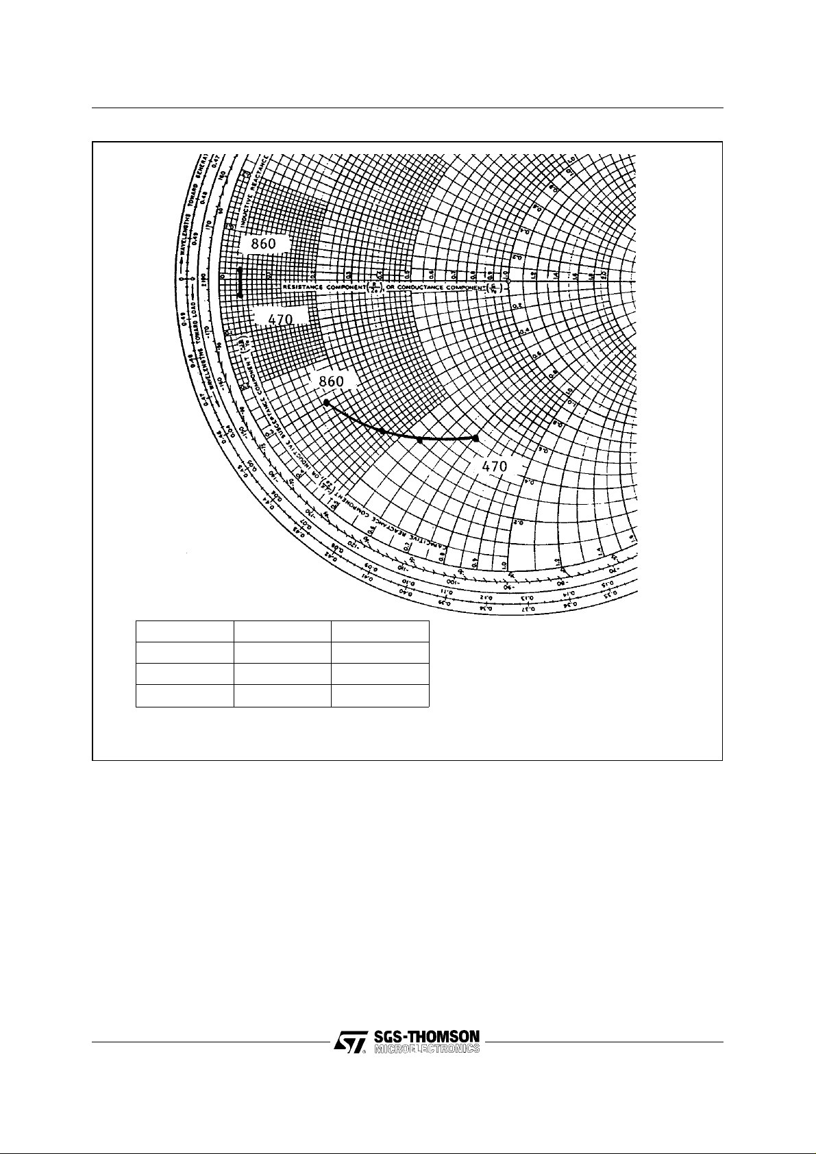
IMPEDANCE DATA
SD1449 (TCC597)
FREQ. ZIN (Ω)Z
OUT
860 MHz 1.8 + j 0.8 8.0 − j 15.0
650 MHz 1.9 − j 0.5 15.0 − j 27.0
470 MHz 2.0 − j 1.5 23.0 − j 35.0
VCC = 20 V
IC = 440 mA
(Ω)
3/4

SD1449 (TCC597)
PACKAGE MECHANICAL DATA
Ref.: Dwg. No.12-0122 rev. B
Informat ion furnishe d is believed to be accur ate and reliable. Ho wever, SGS-THOMS ON Microelectroni cs assumes no responsibility
for the cons equences of us e of such i nformati on nor for a ny infrin gement o f patent s or ot her right s of third p arties w hich may result
from its use. No li cense is gr anted by impl ication or othe rwise under any patent or patent righ ts of SGS-THO MSON Microel ectronics. Specif ications mentioned in thi s publicati on are subject to c hange without notice. This pu blication s upersedes and repl aces all
informati on previou sly supplie d. SGS-THOMS ON Microele ctronics produ cts are not au thorized for us e as critical c omponents in life
support devices or systems without express written approval of SG S-TH OMS ON Micr oelec t roni cs.
©1 994 SGS-TH OMSON Microe lectroni cs - All Rights Res erved
Australia - Brazil - Franc e - Germany - Hong Kong - Italy - Japa n - Korea - Malays ia - Malta - Morocc o - The Netherl ands -
Singapore - Spai n - Sweden - Switz erland - Taiwan - Thailan d - United Kingdo m - U.S.A.
SGS-THOMSON Microelect ronics GR OUP OF C OMPANIES
4/4
 Loading...