

800-960MHz BASE ST ATION APPLICATIONS
.800 - 960 MHz
.24 VOLTS
.EFFICIENCY 50%
.COMMON EMITTER
.GOLD METALLIZATION
.CLASS AB LINEAR OPERATION
.P
OUT
15 W MIN. WITH 8.0 dB GAIN
=
SD1423
RF & MICR OWAVE TRAN SISTOR S
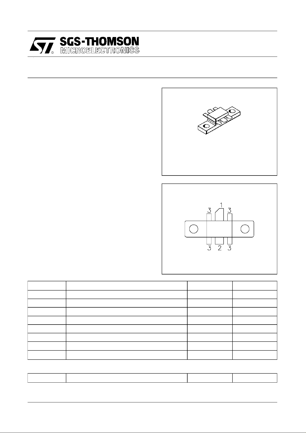
.230 6LFL (M118)
epoxy sealed
OR DER CODE
SD1423
DESCRIP TION
The SD1423 is a gold metallization epitaxial silicon
NPN planar transistor using diffused emitter ballast
resistors for high linearity Class AB operation for
cellular base station applications. The SD1423 is
designed as a medium power output device or as
the driver for the SD1424.
ABSOLUTE MAXIMUM RATINGS (T
Symbol Parameter Value Unit
V
V
V
V
P
T
CBO
CEO
CES
EBO
I
C
DISS
T
J
STG
Collector-BaseVoltage 48 V
Collector-Emitter Voltage 25 V
Collector-Emitter Voltage 45 V
Emitter-Base Voltage 3.5 V
Device Current 2.5 A
Power Dissipation 29 W
Junction Temperature +200
Storage Temperature
case
= 25°C)
PI N CO NNE CTI O N
1. Collector 3. Emitter
2. Base
65 to +150
−
BRANDING
SD1423
°
C
°
C
THERMAL DATA
R
TH(j-c)
August 22, 1996
Junction-CaseThermal Resistance 6
°C/W
1/4
SD 1423
ELECTRICAL SPECI FICATIONS (T
case
STATIC
Symbol Tes t Conditions
BV
CBO I
BV
CEO
BV
I
CBO
h
FE
EBO
= 50mA IE= 0mA
C
IC= 20mA IB= 0mA
IE= 5mA IC= 0mA
VCB= 24V IE= 0mA
VCE= 10V IC= 100mA
DYNAMIC
Symbol Test Conditions
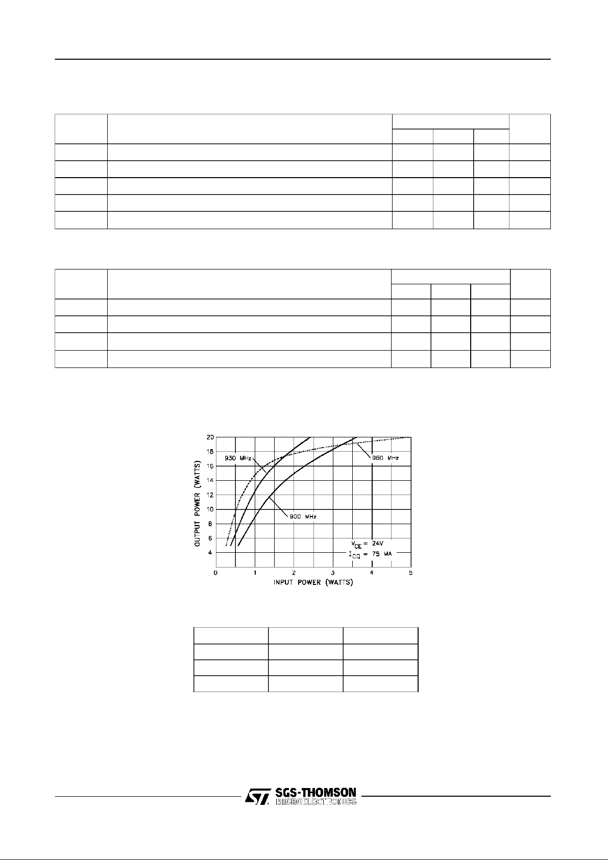
P
OUT f = 960 MHz V
P
η
C
OB
f = 960 MHz VCC= 24 V ICQ= 75 mA
G
cf=960 MHz V
f = 1 MHz VCB= 24V
= 24 V ICQ= 75 mA
CC
= 24 V ICQ= 75 mA
CC
= 25°C)
Value
Min. Typ. Max.
Un it
48 50 — V
25 30 — V
3.5 4.0 — V
— — 1.0 mA
20 — 100 —
Value
Min. Typ. Ma x.
Un it
15 — — W
8——dB
45 50 — %
—2024pF
TYPI CAL PERFORMANCE
IMPEDANCE DATA
P OWER OUTPUT vs POWER INPUT
FREQ.
Z
(Ω)Z
IN
CL
900 MHz 1.30 + j 1.98 3.99 + j 5.55
930 MHz 1.42 + j 2.31 3.18 + j 4.97
960 MHz 1.45 + j 2.62 2.96 + j 4.07
= 15 W
P
OUT
= 75 mA
V
CE
= 24 V
I
CQ
(Ω)
2/4

TEST CI RCUIT
SD1423
C1, C2 :0.8 - 8.0pfGigatrim Variable Capacitor
C3, C6,
C7, C8 :100pf ATC Chip Capacitor
µF, 63V Electrolytic
C4 : 10
C5 : 0.1
µF Capacitor CK06BX104K
D1, D2 :SD1423 trasistors used as diodes
TEST CI RCUIT DI ME NSI ONS
L1, L3 :4 Turn, #22 AWG
L2 : #22 AWG, Ferrite Core
Q1: SD1423 Bias Transistor
Q2: SD1423 transistor under test
R1: 1.5 k
R2: 5K
Board Material: 3M Teflon Fiberglass Er = 2.55, H = .030”
Ω, 1/4W Resistor
Ω ±5% Potentiometer
All dimensions in mils unless otherwise specified
3/4

SD 1423
TEST CI RCUI T LAYOUT
PACKAGE MECHANICAL DATA
Ref.: UDCS Do c. No.1010941 rev. B
Information furnished is believed to be accurate and reliable. However, SGS-THOMSON Microelectronics assumes no responsibility for the
consequences of use of such information nor for any infringement of patents or other rights of third parties which may result from its use.
No license is granted by implication or otherwise under any patent or patent rights of SGS-THOMSON Microelectronics. Specifications
mentioned in this publication are subject to change without notice. This publication supersedes and replaces all information previously
supplied. SGS-THOMSON Microelectronics products are not authorized for use as critical components in life support devices or systems
without express written approval of SGS-THOMSON Microelectronics.
1996 SGS-THOMSON Microelectronics - All Rights Reserved
Australia - Brazil - France - Germany - Hong Kong - Italy - Japan - Korea - Malaysia -
SGS-THOMSON Microelectronics GROUP OF COMPANIES
4/4
 Loading...