

Data Brief
For further information contact your local STMicroelectronics sales office.
May 2007 Rev 1 1/8
8
SABRE-LL-I
Combo motor driver
Features
■ Configurable Device
■ 4 Full Bridges to generate
– Up 2 DC motor drivers and 1 SteppEr
Motor Driver
or
– 4 DC motor drivers
■ Bridges (1 & 2) additional configurations are
– Super DC
– 2 Half Bridges
– 1 super Half Bridge
– 2 switches
–1 super switch
■ Bridges (3 & 4) additional configurations are:
– Same as Bridges 1&2, listed above;
– 2 Buck Regulators (Bridge 3)
– 1 Super Buck Regulator
– Battery Charger (Bridge 4)
■ One variable voltage Buck switching regulator
■ One switching regulator controller
■ One linear regulator
■ Bidirectional serial interface
■ Programmable Watchdog function.
■ Integrated power sequencing and supervisory
functions with fault signaling through serial
interface and external reset pin.
■ Thermal shutdown protection with thermal
warning capability.
■ Very low power dissipation in shut-down mode
(~35 mW)
■ Aux features
– Op amps
–Comparators
– Pass switches
– Multi-channels 9 bit ADC
–GPIOs
Description
SABRe is a new concept of IC in the Motion &
Power Supply field. ST aim is to follow the SABRe
specification and to offer to the customer an IC
with a wide number of features, that can be
configured and customized: Motor Drivers,
Regulators, high precision A/D Converter,
Operational Amplifiers and Voltage Comparators.
The start up configuration can be defined by the
GPIOs and then through the Serial Interface; a
customization can be done through a metal layer
in order to set more complex functions.
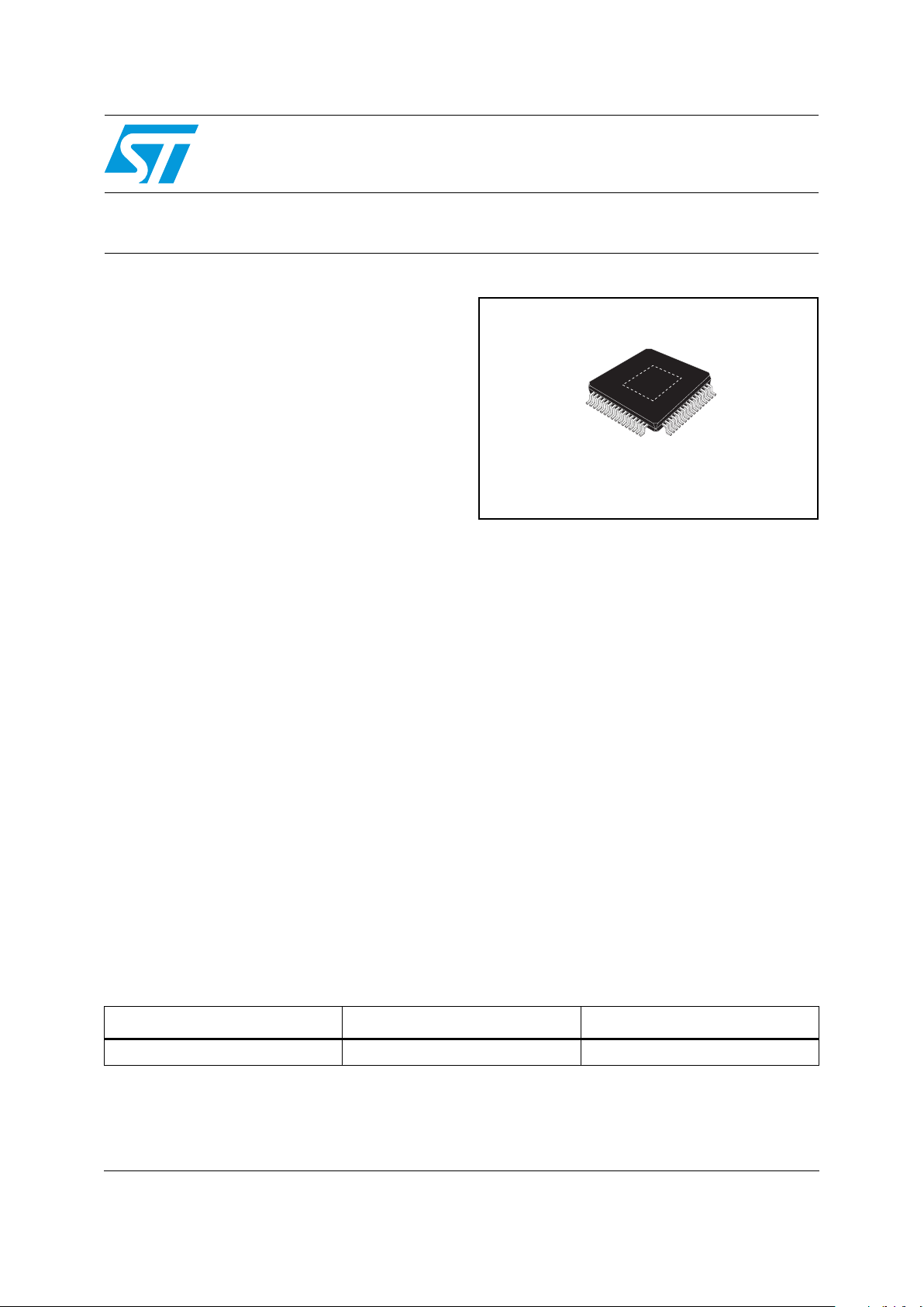
TQFP64 Exposed Pad
Table 1. Device summary
Part number Package Packing
SABRE-LL-I TQFP64 Tray
www.st.com
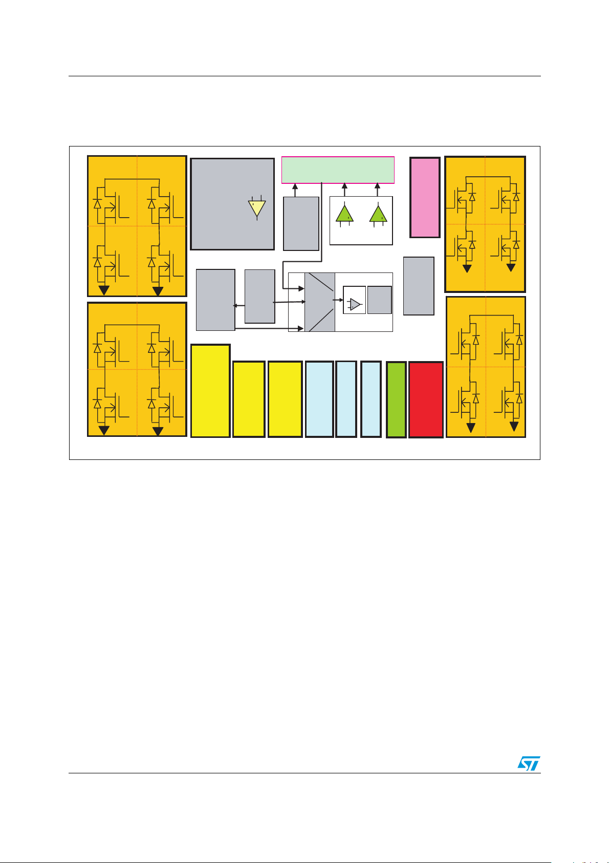
Block diagram SABRE-LL-I
2/8
Block diagram
Figure 1. Block diagram
Main Switching
regulator
Main
Linear
Driver
External FET
Switch Driver
Internal
r
egu
l
a
t
o
r
s
GPIOs
S
P
I
Batt. Charg.
circuitry
Charge Pump
Bridge 2
Bridge 3
Bridge 4
6 bits current Sink
DAC
Bridge 1
ADC
Analog Mux
S/H
(2x)
3.3V
Pass Sw.
Power Up
Sequencer
Supervisory
& Reset
Manager
Thermal
System
V
REF
=1V
SSAABBRRee
Switching reg.
controller
Int. Ref. Volt
Op Amps
AC0019
9

SABRE-LL-I Detailed description
3/8
Detailed description
● Four widely configurable Full Bridges. Diagonal R
dson
are:
– Bridge 1 and 2:
– Diagonal Rdson: 1.1Ω;
– Max operative current= 2.5A.
– Bridge 3 and 4:
– Diagonal Rdson: 1.6Ω;
– Max operative current= 1.5A.
The possible configurations for each bridge are the following:
– Bridge 1 or 2:
– DC motor driver
– Super DC (Bridge 1 and 2 paralleled form SuperBridge1)
– 2 Half Bridges
– 1 super Half Bridge
– 2 switches
– 1 super switch
– Bridge 3 has the same configurations as Bridge 1 or 2 (Bridge 3 and 4 paralleled they
form SuperBridge2) plus the following:
– ½ Stepper motor driver
– 2 Buck regulators (V
AUX1_SW
, V
AUX2_SW
)
– 1 super Buck regulator
– Bridge 4 has the same configurations as Bridge 1 or 2 (Bridge 4 and 3 paralleled they
form SuperBridge2) plus the following:
– ½ Stepper motor driver
– 1 Super Buck regulator (VAUX3_SW)
– Battery charger
● One variable voltage Buck switching regulator (V
MAIN_SW
) with:
– Internal soft start sequence.
– Pulse skipping strategy control.
– Internal PWM generation.
– Internal power FET.
– Regulated voltage range: 1-5 Volts.
– Output load current: 3.0 A.
– Switching frequency: ~250KHz.
● One switching regulator controller (V
EXT_SW
) with:
– Pulse skipping strategy control.
– Internal PWM generation.
– Regulated voltage range: 1-30 Volts.
– Current limitation.

Detailed description SABRE-LL-I
4/8
● One linear regulator (V
MAIN_LIN
) that can be used to generate low current low ripple
voltages. This regulator can be used to drive an external bipolar pass transistor to
generate high current/low ripple output voltage.
● Current sink DAC:
– 64 available current levels (6 bits programmable).
– Up to 64 mA output current.
– 5 Volt tolerant.
● Two Operational Amplifiers:
– 3.3V supply, rail to rail input compatibility, internally compensated.
– They can have all pins externally accessible or can be internally configured as a
buffer, for internal reference voltages.
– Unity Gain Bandwidth > 1MHz.
● Two Comparators with 3.3V input compatibility and low offset.
● Two 3.3V Pass Switches with 1Ω R
dson
and short circuit protected.
● One 8bits/9bits A/D converter (100KS/sec @ 9 bits, 200KS/sec @8bits). It can be used
to measure most of the internal signals, of the input pins and the IC temperature.
● Fourteen General Purpose I/Os that can be used to drive/read internal/external
analog/logic signals.
● Bidirectional Serial Interface with address detection so that different ICs can share the
same data-bus.
● Programmable Watchdog function.
● Integrated power sequencing and supervisory functions with fault signaling through
serial interface and external reset pin.
● Thermal shutdown protection with thermal warning capability.
● Very Low power dissipation in Shut-down mode (~35 mW)
● SABRe is intended to maximize the use of its components, so that when an internal
circuit is not needed it could be used for other applications. Bridge 3, for example, can
be used as a bridge or to implement two switching regulators with synchronous
rectification: to obtain this flexibility SABRe includes 2 separate regulation loops for
these regulators. When the bridge is used as a motor driver, the 2 regulation loops can
be redirected on general purpose I/Os, to leave the possibility to assembly a switching
regulator using an external FET and one of these regulation loops.

SABRE-LL-I Global specifications
5/8
Global specifications
Absolute maximum specifications
The following specifications define the maximum range of voltages or currents for SABRe.
Stresses above these Absolute Maximum specifications may cause permanent damage to
the device.
Exposure to Absolute Maximum Ratings for extended periods may affect device reliability.
Operating ratings specifications
Table 2. Absolute maximum ratings
Symbol Parameters Conditions Min. Max Unit
V
Supply_Abs
Maximum supply voltage 40 V
V
3V3pin_Abs
3.3V pins maximum input
voltage
3.9 V
V
Sw_Abs
Switching regulators
output pin voltage range.
-3 V
Supply
V
V
Pump_Abs
Charge pump pins max
voltage.
(1)
1. This value is useful to define the voltage rating for an external capacitor to be connected from VSupply to
VPump.
VPump is internally generated and can never be supplied by an external voltage source nor, is it intended to
provide voltage to external loads.
TBD V
T
j_Abs
Junction temperature
(2)
2. TSD means the "Thermal Shut Down" temperature of the device.
Storage -40 190 °C
Operating 0 TSD °C
Table 3. IC operating ratings
Symbol Characteristic Conditions Min Max Unit
V
Supply_Op
Supply voltage range 23 38 V
I
Supply_Op
Operative supply current
(1)
1. Operating supply current is measured with System regulators operating but externally loaded only with the
specified minimum load.
15 mA
I
Shut_down
Shut down state supply
current
1mA
V
3V3pin_Op
3.3 volt pins max voltage 3.6 V
T
j_Abs
Junction temperature Operating 0 125. °C

Package information SABRE-LL-I
6/8
Package information
In order to meet environmental requirements, ST offers these devices in ECOPACK®
packages. These packages have a Lead-free second level interconnect. The category of
second Level Interconnect is marked on the package and on the inner box label, in
compliance with JEDEC Standard JESD97. The maximum ratings related to soldering
conditions are also marked on the inner box label.
ECOPACK is an ST trademark. ECOPACK specifications are available at: www.st.com.
Figure 2. TQFP64 mechanical data and package dimensions
OUTLINE AND
MECHANICAL DATA
DIM.
mm inch
MIN. TYP. MAX. MIN. TYP. MAX.
A 1.20 0.0472
A1 0.05 0.15 0.002 0.006
A2 0.95 1.00 1.05 0.0374 0.0393 0.0413
b 0.17 0.22 0.27 0.0066 0.0086 0.0086
c 0.09 0.20 0.0035 0.0078
D 11.80 12.00 12.20 0.464 0.472 0.480
D1 9.80 10.00 10.20 0.386 0.394 0.401
D2 2.00 0.787
D3 7.50 0.295
E 11.80 12.00 12.20 0.464 0.472 0.480
E1 9.80 10.00 10.20 0.386 0.394 0.401
E2 2.00 0.787
E3 7.50 0.295
e 0.50 0.0197
L 0.45 0.60 0.75 0.0177 0.0236 0.0295
L1 1.00 0.0393
k 0˚3.5˚7˚ 0˚3.5˚7˚
ccc 0.080 0.0031
TQFP64 (10x10x1.0mm)
Exposed Pad Down
7278840 B

SABRE-LL-I Revision history
7/8
Revision history
Table 4. Document revision history
Date Revision Changes
3-May-2007 1 Initial release.

SABRE-LL-I
8/8
Please Read Carefully:
Information in this document is provided solely in connection with ST products. STMicroelectronics NV and its subsidiaries (“ST”) reserve the
right to make changes, corrections, modifications or improvements, to this document, and the products and services described herein at any
time, without notice.
All ST products are sold pursuant to ST’s terms and conditions of sale.
Purchasers are solely responsible for the choice, selection and use of the ST products and services described herein, and ST assumes no
liability whatsoever relating to the choice, selection or use of the ST products and services described herein.
No license, express or implied, by estoppel or otherwise, to any intellectual property rights is granted under this document. If any part of this
document refers to any third party products or services it shall not be deemed a license grant by ST for the use of such third party products
or services, or any intellectual property contained therein or considered as a warranty covering the use in any manner whatsoever of such
third party products or services or any intellectual property contained therein.
UNLESS OTHERWISE SET FORTH IN ST’S TERMS AND CONDITIONS OF SALE ST DISCLAIMS ANY EXPRESS OR IMPLIED
WARRANTY WITH RESPECT TO THE USE AND/OR SALE OF ST PRODUCTS INCLUDING WITHOUT LIMITATION IMPLIED
WARRANTIES OF MERCHANTABILITY, FITNESS FOR A PARTICULAR PURPOSE (AND THEIR EQUIVALENTS UNDER THE LAWS
OF ANY JURISDICTION), OR INFRINGEMENT OF ANY PATENT, COPYRIGHT OR OTHER INTELLECTUAL PROPERTY RIGHT.
UNLESS EXPRESSLY APPROVED IN WRITING BY AN AUTHORIZED ST REPRESENTATIVE, ST PRODUCTS ARE NOT
RECOMMENDED, AUTHORIZED OR WARRANTED FOR USE IN MILITARY, AIR CRAFT, SPACE, LIFE SAVING, OR LIFE SUSTAINING
APPLICATIONS, NOR IN PRODUCTS OR SYSTEMS WHERE FAILURE OR MALFUNCTION MAY RESULT IN PERSONAL INJURY,
DEATH, OR SEVERE PROPERTY OR ENVIRONMENTAL DAMAGE. ST PRODUCTS WHICH ARE NOT SPECIFIED AS "AUTOMOTIVE
GRADE" MAY ONLY BE USED IN AUTOMOTIVE APPLICATIONS AT USER’S OWN RISK.
Resale of ST products with provisions different from the statements and/or technical features set forth in this document shall immediately void
any warranty granted by ST for the ST product or service described herein and shall not create or extend in any manner whatsoever, any
liability of ST.
ST and the ST logo are trademarks or registered trademarks of ST in various countries.
Information in this document supersedes and replaces all information previously supplied.
The ST logo is a registered trademark of STMicroelectronics. All other names are the property of their respective owners.
© 2007 STMicroelectronics - All rights reserved
STMicroelectronics group of companies
Australia - Belgium - Brazil - Canada - China - Czech Republic - Finland - France - Germany - Hong Kong - India - Israel - Italy - Japan -
Malaysia - Malta - Morocco - Singapore - Spain - Sweden - Switzerland - United Kingdom - United States of America
www.st.com
 Loading...