


RBO40-40G/M/T
ApplicationSpecific Discretes
A.S.D.
FEATURES
PROTECTIONAGAINST”LOADDUMP”PULSE
40A DIODE TO GUARD AGAINST BATTERY
REVERSAL
MONOLITHIC STRUCTURE FOR GREATER
RELIABILITY
BREAKDOWNVOLTAGE: 24V min.
CLAMPINGVOLTAGE: ± 40V max.
COMPLIANTWITHISO /DTR 7637
DESCRIPTION
Designedto protectagainst batteryreversaland
loaddumpovervoltagesin automotiveapplications,thismonolithiccomponentoffersmultiple
functionsin thesamepackage:
D1 : reversedbatteryprotection
T1 : clampingagainst negativeovervoltages
T2 : Transilfunctionagainst ”loaddump” effect.
TM
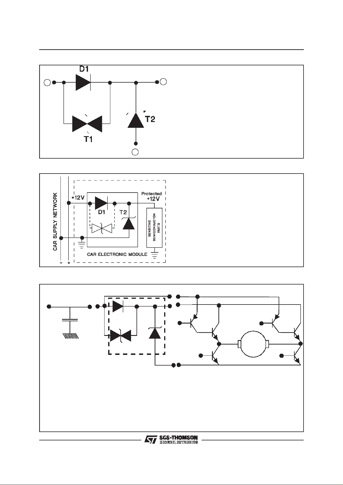
OVERVOL TAGEPROTECTIO NCIRCUIT(R BO)
REVERSEDBATTERYAND
D2PAK
RBO40-40G
PowerSO-10
RBO40-40M
TM
January1997 -Ed :3
TO220AB
RBO40-40T
FUNCTIONAL DIAGRAM
1
3
2
1/15

RBO40-40G / RBO40-40M / RBO40-40T
ABSOLUTE MAXIMUM RATINGS
Symbol Parameter Value Unit
I
FSM
Non repetitivesurgepeak forward current
tp = 10ms 120 A
(DiodeD1)
I
F
V
PP
DC forwardcurrent (Diode D1) Tc = 75°C40 A
Peakload dump voltage (seenote 1and2)
80 V
5 pulses(1 minute between each pulse)
P
PP
Peakpulse power betweenInput andOutput
10/1000µs 1500 W
(TransilT1) Tj initial= 25°C
T
stg
Tj
T
L
Storagetemperature range
Maximumjunction temperature
Maximumlead temperatureforsolderingduring 10 s
- 40 to + 150
150
260 °C
at 4.5mm from casefor TO220AB
Note 1 :for a surge greater than the maximum value, the device will fail in short-circuit.
Note 2 : see Load Dump curves.
TM : PowerSO-10,TRANSIL and ASD are trademarks of SGS-THOMSON Microelectronics.
THERMAL RESISTANCE
Symbol Parameter Value Unit
Rth (j-c)
Junctionto case
RBO40-40M
RBO40-40G
RBO40-40T
1.0
1.0
1.0
°C
°C/W
Rth (j-a) Junctionto ambient RBO40-40T 60 °C/W
D1
I13
31
F
I
T1
V
31 VRM31
CL
Ex: VF13 . betweenPin 1andPin3 VBR32. between Pin 3 and Pin 2
T2
2
V
31
BR
V
IRM31
31
I
R
Ipp31
F13
V13
Ipp32
I
RM
I32
IR32
32
VRM32 V
32 V
R
B
1
V32
32
C
L
3
2
2/15
RBO40-40G / RBO40-40M / RBO40-40T
Symbol Parameter
V
RM31/VRM32
V
BR31/VBR32
I
R31/IR32
V
CL31/VCL32
V
F13
I
PP
αT Temperaturecoefficientof V
C
31/C32
C
13
Stand-offvoltage Transil T1/ Transil T2.
Breakdownvoltage Transil T1 / TransilT2.
LeakagecurrentTransilT1 /TransilT2.
ClampingvoltageTransilT1 /TransilT2.
Forwardvoltagedrop DiodeD1.
Peak pulse current.
.
BR
CapacitanceTransil T1/ TransilT2.
Capacitanceof DiodeD1
ELECTRICAL CHARACTERISTICS: DIODED1 (-40°C< T
amb
Symbol Test Conditions
V
V
V
V
C
F13
F13
F13
F13
13
IF= 40A 1.9 V
IF= 20A 1.45 V
IF=1A 1 V
IF= 100mA
F = 1MHz VR=0V
ELECTRICAL CHARACTERISTICS: TRANSILT1 (- 40°C<T
Symbol Test Conditions
V
BR 31
V
BR 31
I
RM 31
I
RM 31
V
CL 31
αT Temperaturecoefficient of V
C
31
IR=1 mA 22 35 V
IR=1 mA,T
=25°C2432V
amb
VRM=20 V 100 µA
VRM=20V,T
amb
=25°C
IPP=37.5A,Tjinitial= 25° C 10/1000µs40V
BR
F = 1MHz VR= 0 V 3000 pF
<+85°C)
<+85°C)
amb
Value
Min. Typ. Max.
0.95 V
3000 pF
Value
Min. Typ. Max.
10 µA
910-4/°C
Unit
Unit
ELECTRICAL CHARACTERISTICS : TRANSILT2 (- 40°C<T
Symbol Test Conditions
V
BR 32
V
BR 32
I
RM 32
I
RM 32
V
CL 32
α T Temperaturecoefficientof V
C
32
Note 1 : One pulse,see pulse definition in load dump testgenerator circuit.
IR=1 mA 22 35 V
IR=1 mA,T
=25°C2432V
amb
VRM=20 V 100 µA
VRM=20V,T
amb
=25°C
IPP= 20 A (note1) 40 V
BR
F = 1MHz VR=0 V 8000 pF
amb
<+85°C)
Value
Min. Typ. Max.
Unit
10 µA
910-4/°C
3/15
RBO40-40G / RBO40-40M / RBO40-40T
PRODUCTDESCRIPTION
1
2
BASICAPPLICATION
TheRBO has 3functionsintegratedonthe same
chip.
3
D1 : “Diode function” in order to protect against
reversedbattery operation.
T2: “Transil function” in order to protectagainst
positive surge generated by electric systems
(ignition,relay. ...).
T1: Protectionformotor drive application
(Seebelow).
* The monolithic multi-function protection
(RBO) has been developed to protect
sensitivesemiconductorsin car electron ic
modules against both overvoltage and
batteryreverse.
* In addition, the RBO circuit prevents
overvoltages generated by the module from
affecting the carsupply network.
MOTORDRIVER APPLICATION
BATTERY
Filter
D1
T2
T1
MOTOR
RBO
DEVIC E MOTO R C ONTROL
In thisapplication,onehalfof the motordrivecircuitis suppliedthroughthe “RBO” and isthusprotected
as perits basicfunctionapplication.
The secondpart isconnecteddirectly to the“carsupplynetwork” and is protectedas follows:
- Forpositivesurges: T2(clampingphase)and D1in forward-biased.
- Fornegativesurges: T1(clampingphase) andT2 inforward-biased.
4/15

2
PINOUTconfigurationin D
PAK:
-Input (1) : Pin1
-Output (3) : Pin3
-Gnd (2) : Connectedto base Tab
Marking : Logo,datecode, RBO40-40G
PINOUTconfigurationin PowerSO-10:
-Input (1) : Pin1 to 5
-Output (3) : Pin6 to10
-Gnd (2) : Connectedto base Tab
Marking : Logo,datecode, RBO40-40M
RBO40-40G / RBO40-40M / RBO40-40T
D1
T2
T1
TAB
Pin 1
D1
Input (1)
Output (3)
T2
T1
Gnd (2)
Tab
Pin 6
PINOUTconfigurationin TO220AB:
-Input (1) : Pin1
-Output (3) : Pin3
-GND (2) : Connectedto baseTab
Marking : Logo,datecode, RBO40-40T
TOP VIEW
D1
T2
T1
(TAB)
5/15

RBO40-40G / RBO40-40M / RBO40-40T
LOADDUMP TESTGENERATORCIRCUIT (SCHAFFNER NSG506 C).Issued from ISO / DTR7637.
U(V)
Vbat
Open circuit (voltage curve)
Corresponding current wave with D.U.T.
(pulse test n°5)
I
Ipp
Ipp/2
90%
Vs
t
tr
offset
10% / 13.5V
10%
0
t
0
tp = 40ms
t
Impulse N°5
Vs(V) 66.5
Vbat(V) 13.5
Ri (Ω)2
t (ms)
200 (*)
tr (ms) <10
Number 5
60s between each pulse
(*) Generator setting
CALIBRATION METHODFOR SCHAFFNERNSG 506 C
1) With opencircuit (generatoris inopencircuit):
- calibrateVs
2) With shortcircuit(generatorisin shortcircuit):
-calibrateRi (Ri = 2Ω)
3) With D.U.T.
- calibratetp (tp= 40ms @ Ipp/2)
TypicalVoltage curve (open circuit)
typ. Vpp
V
Bat
20ms/div.
10.0V/div.
Typical Voltage andCurrent curvewith D.U.T.
typ.VCL
Ipp
20ms/div.
5.0V/div.
20ms/div.
3A/div.
6/15

RBO40-40G / RBO40-40M / RBO40-40T
Fig. 1 : Peak pulse power versus exponential
pulseduration(Tjinitial = 85°C).
Ppp(kW)
10.0
5.0
2.0
1.0
0.5
0.2
0.1
12 51020 50100
Transil T1
Tra nsil T 2
tp(ms)
Fig. 2-2 : Clamping voltage versus peak pulse
current (Tj initial = 85°C).
Exponential waveform tp = 1 ms and tp = 20 µs
(TRANSILT1).
Fig. 2-1 : Clamping voltage versus peak pulse
current (Tj initial = 85°C).
Exponential waveform tp = 40 ms and tp = 1 ms
(TRANSILT2).
V (V)CL
45.0
42.5
40.0
37.5
35.0
32.5
30.0
0.2 0.5 1 2 5 10 20 50 100
0.1
tp = 40ms
tp = 1ms
Ipp(A)
Fig. 3 : Relative variation of peak pulse power
versus junction temperature.
V (V)CL
55
50
45
p=1ms
40
t
tp = 20µs
35
30
A)
25
1 2 5 10 20 50 100 200 500
Ipp(
Ppp[Tj]/Ppp[Tj initial=85°C]
1.20
1.00
0.80
0.60
0.40
0.20
0.00
25 50 75 100 125 150 175
0
Tj initial (°C)
7/15

RBO40-40G / RBO40-40M / RBO40-40T
Fig. 4 :
Relative variation of thermal impedance
junctionto caseversuspulse duration.
Zth(j-c)/Rth(j-c)
1.0
0.5
0.2
0.1
1E-3 1E-2 1E-1 1E+0 1E+1
Fig. 5-2 :
Peak forwardvoltage drop versus peak
tp (s)
forwardcurrent(typicalvalues)- (DIODED1).
Fig. 5-1 :
Peakforward voltagedrop versus peak
forwardcurrent (typicalvalues) -(TRANSILT2).
V
FM(V)
2.0
1.8
1.6
1.4
1.2
1.0
0.8
0.6
0.4
0.1 0.2 0.5 1 2
Tj = 25°°C
Tj = 150°°C
5
10 20 50 100
IFM(A)
Fig.6 :Relative variation of leakage current
versus junction temperature.
V
FM(V)
3.5
3.5
3.0
3.0
2.5
2.5
2.0
2.0
1.5
1.5
1.0
1.0
0.5
0.5
0.2 0.5 1 5 20 50 100
0.2 0.5 2 1020 50100
0.1
0.1
Tj = 25°°C
Tj = 150°°C
ORDERINGINFORMATION
RBO 40 - 40 M
ReversedBattery&
Overvoltageprotection
IFM(A)
Package:
M = PowerSO-10
2
G=D
PAK
T =TO220AB
8/15
I
F(AV)
=40A
=40V
V
CL

PACKAGEMECHANICAL DATA
2
PAK Plastic
D
E
L2
L
L3
A1
B2
B
G
2.0 MIN.
FLATZONE
C2
RBO40-40G / RBO40-40M / RBO40-40T
DIMENSIONS
A
A 4.30 4.60 0.169 0.181
A1 2.49 2.69 0.098 0.106
A2 0.03 0.23 0.001 0.009
REF.
D
B 0.70 0.93 0.027 0.037
B2 1.40 0.055
C 0.45 0.60 0.017 0.024
C2 1.21 1.36 0.047 0.054
C
R
D 8.95 9.35 0.352 0.368
E 10.00 10.28 0.393 0.405
G 4.88 5.28 0.192 0.208
L 15.00 15.85 0.590 0.624
A2
L2 1.27 1.40 0.050 0.055
L3 1.40 1.75 0.055 0.069
R 0.40 0.016
V2
V2 0° 8° 0° 8°
Millimeters Inches
Min. Typ. Max. Min. Typ. Max.
FOOT-PRINT D
10.30
2
PAK
8.90
16.90
5.08
1.30
3.70
9/15

RBO40-40G / RBO40-40M / RBO40-40T
SOLDERINGRECOMMENDATION
The soldering process causes considerable
thermal stress to a semiconductor component.
This has to be minimized to assure a reliable and
extended lifetime of thedevice. The PowerSO-10
package can be exposed to a maximum
temperatureof 260°C for 10 seconds. However a
proper solderingof the packagecould be done at
215°C for 3 seconds. Any solder temperature
profile should be within these limits. As reflow
techniquesaremost commonin surfacemounting,
typical heating profilesare given in Figure 1,either
for mounting on FR4 or on metal-backed boards.
For each particular board, the appropriate heat
profile has to be adjusted experimentally. The
present proposal is just a starting point. In any
case, the following precautions have to be
considered:
- alwayspreheatthe device
- peak temperatureshould beat least30 °C
higherthanthe meltingpoint of thesolder
alloychosen
Fig. 1 :Typicalreflowsolderingheat profile
-thermalcapacityof thebase substrate
Voids pose a difficult reliability problem for large
surface mount devices. Such voids under the
package result in poor thermal contact and the
high thermal resistance leads to component
failures. The PowerSO-10 is designed from
scratch to be solely a surface mount package,
hence symmetry in the x- and y-axis gives the
package excellent weight balance.Moreover, the
PowerSO-10offersthe uniquepossibilityto control
easily the flatness and quality of the soldering
process. Both the top and the bottom soldered
edges of the package are accessible for visual
inspection(soldering meniscus).
Coplanarity between the substrate and the
package can be easily verified. The quality of the
solder joints is very importantfor two reasons : (I)
poor quality solder joints result directly in poor
reliability and (II) solder thickness affects the
thermal resistance significantly. Thus a tight
control of this parameter results in thermally
efficientandreliablesolder joints.
Temperature ( C)
250
o
o
245 C
o
215 C
200
Soldering
Cooli ng
150
Epoxy FR4
board
Preheating
100
Metal-backed
50
board
0
0 40 8 0 1 20 160 2 00 2 40 280 320 360
Time (s )
10/15

RBO40-40G / RBO40-40M / RBO40-40T
SUBSTRATESAND MOUNTINGINFORMATION
The use of epoxy FR4 boardsis quite commonfor
surface mounting techniques,however, their poor
thermal conductioncompromisesthe otherwise
outstanding thermal performance of the
PowerSO-10. Some methods to overcome this
limitationare discussedbelow.
One possibilityto improve the thermal conduction
is the use of large heat spreader areas at the
copper layer of the PC board. This leads to a
reductionof thermal resistanceto 35 °C for 6 cm
of theboard heatsink(seefig.2).
Use of copper-filledthroughholes on conventional
FR4 techniqueswillincrease the metallization and
Fig.2 :
Mountingon epoxyFR4head dissipationby extendingthe area ofthecopper layer
Copper foil
decrease thermal resistance accordingly. Using
a configurationwith 16holesunderthe spreaderof
the packagewith apitch of 1.8mm and a diameter
of 0.7 mm, the thermal resistance (junction heatsink) can be reduced to 12°C/W (see fig. 3).
Besidethe thermaladvantage, thissolutionallows
multi-layer boards to be used. However, a
drawback of this traditional material prevents its
use in very high power, high current circuits. For
instance, it is not advisable to surface mount
devices with currents greater than 10 A on FR4
2
boards. A Power Mosfet or Schottky diode in a
surfacemount power packagecan handleup to
around50 A ifbetter substratesare used.
FR4 board
Fig. 3 :
Mountingon epoxyFR4 byusing copper-filledthroughholesfor heattransfer
Copperfoil
heattransferheatsink
FR4board
11/15

RBO40-40G / RBO40-40M / RBO40-40T
A new technology available today is IMS - an
Insulated Metallic Substrate. This offers greatly
enhanced thermal characteristics for surface
mount components.IMS is a substrateconsisting
of threedifferentlayers,(I) thebasematerialwhich
is availableas an aluminiumor a copperplate, (II)
a thermal conductive dielectrical layer and (III) a
copper foil, whichcan be etched as a circuitlayer.
Using this material a thermalresistance of 8°C/W
with 40 cm
2
of board floating in air is achievable
(seefig. 4). If evenhigherpower is to bedissipated
an externalheatsink couldbe appliedwhich leads
to an R
that R
(j-a) of 3.5°C/W (see Fig. 5), assuming
th
(heatsink-air) is equal to R
th
(junction-heatsink). This is commonly applied in
practice, leading to reasonable heatsink
dimensions. Often power devices are defined by
Fig.4 :Mountingon metalbacked board
Copper foil
Insulation
consideringthe maximumjunction temperatureof
the device. In practice , however, this is far from
being exploited. A summary of various power
managementcapabilities is madein table1 based
on a reasonabledeltaT of70°Cjunctionto air.
The PowerSO-10 concept also represents an
attractive alternati ve to C.O.B. techniques.
PowerSO-10 offers devices fully tested at low
and high temperature. Mounting is simple - only
conventionalSMT isrequired - enabling the users
togetrid ofbondwire problemsand theproblemto
controlthe hightemperaturesoftsolderingas well.
An optimized thermal managementis guaranteed
th
through PowerSO-10 as the power chips must in
any case be mounted on heat spreaders before
beingmountedonto the substrate.
Fig. 5 :
Mounting on metal backed board with an
externalheatsinkapplied
Copper foil
FR4board
Alumini um
Aluminium
heatsink
TABLE1
PowerSo-10packagemountedon Rth(j-a) PDiss
1.FR4using the recommendedpad-layout
2
2.FR4withheatsink on board(6cm
)35°C/W 2.0 W
50 °C/W 1.5 W
3.FR4withcopper-filledthroughholes andexternalheatsink applied 12 °C/W 5.8 W
4. IMS floating inair (40cm
5. IMS with externalheatsinkapplied
2
)8°C/W 8.8 W
3.5 °C/W 20 W
12/15

PACKAGEMECHANICAL DATA
RBO40-40G / RBO40-40M / RBO40-40T
B
H
A1
Q
0.10A B
E3 E1
SEATING
PLANE
A
C
10
E
1
eB
0.25 M
6
E2
5
DETAIL”A”
D
h
D1
A
F
SEATING
PLANE
A1
L
DETAIL”A”
a
E4
DIMENSIONS
REF.
Millimeters Inches
Min. Typ. Max. Min. Typ. Max.
A 3.35 3.65 0.131 0.143
A1 0.00 0.10 0.00 0.0039
B 0.40 0.60 0.0157 0.0236
C 0.35 0.55 0.0137 0.0217
D 9.40 9.60 0.370 0.378
D1 7.40 7.60 0.291 0.299
E 9.30 9.50 0.366 0.374
E1 7.20 7.40 0.283 0.291
E2 7.20 7.60 0.283 0.299
DIMENSIONS
REF.
Millimeters Inches
Min. Typ. Max. Min. Typ. Max.
E3 6.10 6.35 0.240 0.250
E4 5.90 6.10 0.232 0.240
e 1.27 0.05
F 1.25 1.35 0.0492 0.0531
H 13.80 14.40 0.543 0.567
h 0.50 0.019
L 1.20 1.80 0.0472 0.0708
Q 1.70 0.067
a0° 8°0° 8°
13/15

RBO40-40G / RBO40-40M / RBO40-40T
FOOTPRINT
MOUNTINGPAD LAYOUT
RECOMMENDED
Dimensionsin millimeters Dimensionsin millimeters
HEADERSHAPE
SHIPPINGTUBE
C
B
A
Surfacemount film taping: contactsales office
A
B
C
Lengthtube
Quantityper tube
DIMENSIONS(mm)
TYP
18
12
0,8
532
50
14/15

PACKAGEMECHANICALDATA
TO220AB Plastic
RBO40-40G / RBO40-40M / RBO40-40T
DIMENSIONS
REF.
A 14.23 15.87 0.560 0.625
a1 4.50 0.177
a2 12.70 14.70 0.500 0.579
B 10.20 10.45 0.402 0.411
b1 0.64 0.96 0.025 0.038
b2 1.15 1.39 0.045 0.055
C 4.48 4.82 0.176 0.190
c1 0.35 0.65 0.020 0.026
c2 2.10 2.70 0.083 0.106
e 2.29 2.79 0.090 0.110
F 5.85 6.85 0.230 0.270
I 3.55 4.00 0.140 0.157
L 2.54 3.00 0.100 0.118
l2 1.45 1.75 0.057 0.069
l3 0.80 1.20 0.031 0.047
Millimeters Inches
Min. Max. Min. Max.
Information furnished is believedto be accurate and reliable. However, SGS-THOMSON Microelectronics assumes no responsibility forthe
consequences of use of such information nor for any infringement of patents or other rights of third parties which may result fromits use.No
license is grantedby implicationor otherwise under any patent or patentrights of SGS-THOMSON Microelectronics.Specifications mentioned
in this publication are subjectto change withoutnotice. This publication supersedes andreplaces all informationpreviously supplied.
SGS-THOMSONMicroelectronics productsare notauthorized foruse as criticalcomponents in life support devices or systems without express
written approval of SGS-THOMSONMicroelectronics.
1997SGS-THOMSON Microelectronics -Printed inItaly - All rights reserved.
SGS-THOMSON MicroelectronicsGROUP OF COMPANIES
Australia- Brazil- Canada - China- France- Germany- Italy - Japan -Korea -Malaysia - Malta - Morocco
The Netherlands - Singapore - Spain- Sweden - Switzerland - Taiwan- Thailand - United Kingdom -U.S.A.
15/15
 Loading...