

FAST RECOVERY RECTIFIER DIODES
VERY FAST FORWARD AND REVERSE
RECOVERY DIODES
SUITABLE APPLICATION
SWTCHING POWER TRANSISTORS DRIVER
CIRCUITS (SERIES DIODES IN
ANTISATURATION CLAM P SP EED U P D IODE
IN DISCRETE DARLINGTON...)
THYRISTORS GATE DRIVER CIRCUITS
HIGH FREQUENCY RECTIFICATION
PLQ 08
PLQ 1
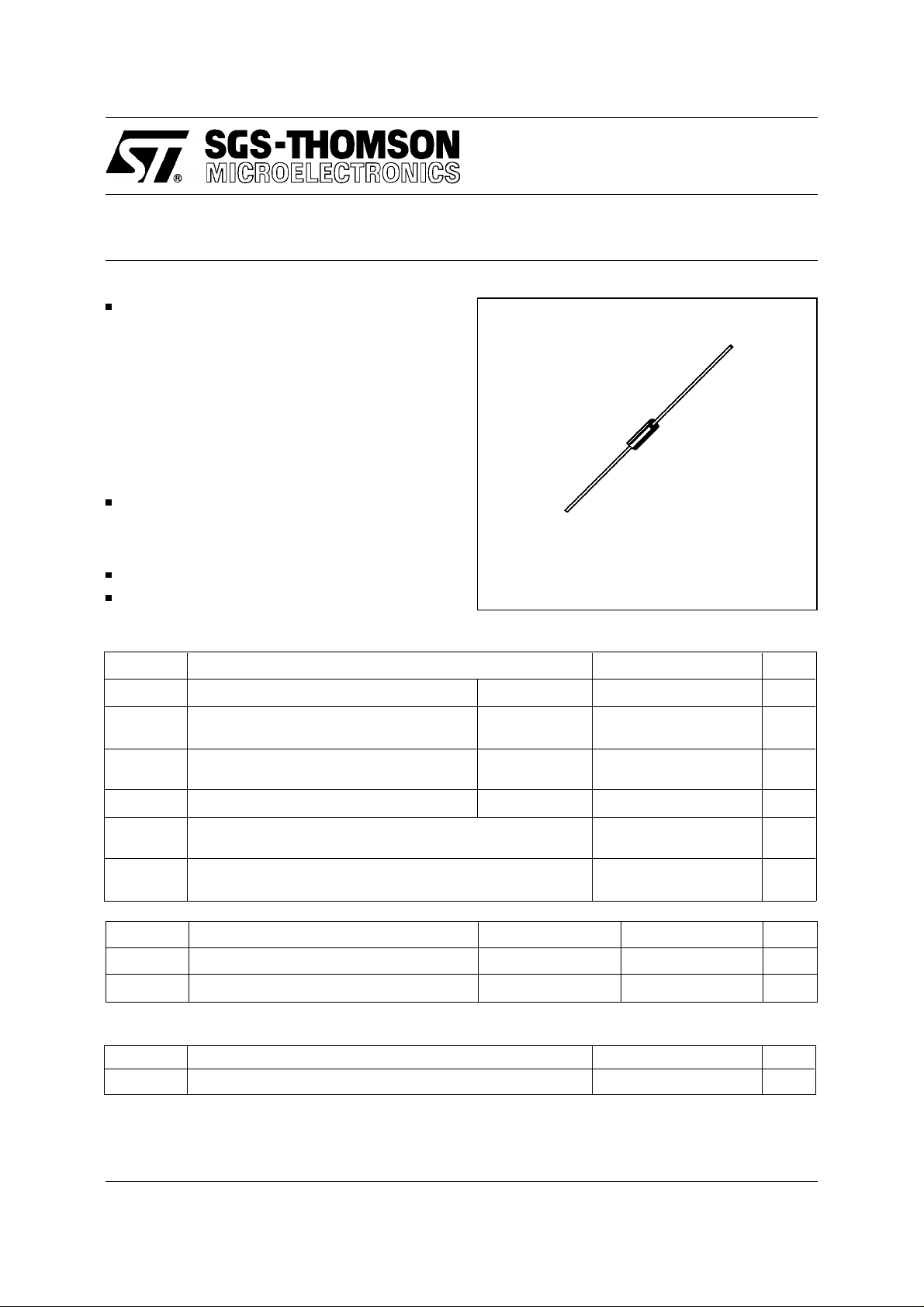
F 126
(Plastic)
ABSOLUTE RATINGS (limiting values)
Symbol Parameter Value Unit
I
FRM
I
F (AV)
I
FSM
P
tot
T
stg
T
T
L
Symbol Parameter PLQ 08 PLQ 1 Unit
V
RRM
V
RSM
Repetive Peak Forward Current
Average Forward Current* Ta = 25°C
Surge non Repetitive Forward Current tp = 10ms
Power Dissipation*
Storage and Junction Temperature Range - 40 to 125
j
Maximum Lead Temperature for Soldering during 10s at 4mm
from Case
Repetitive Peak Reverse Voltage 80 100 V
Non Repetitive Peak Reverse Voltage 80 100 V
≤ 20µs
t
p
δ = 0.5
Sinusoidal
Ta = 25°C
20 A
1A
20 A
1.7 W
230
THERMAL RESISTANCE
Symbol Parameter Value Unit
R
th (j - a)
Junction-ambient* 60
°C
°C
°C/W
* On infinite heatsink with 10mm lead length.
November 1994
1/5

PLQ 08/PLQ 1
ELECTRICAL CHARACTERISTICS
STATIC CHARACTERISTICS
Synbol Test Conditions Min. Typ. Max. Unit
I
R
V
F
Tj = 25°C
= 100°C
T
j
Tj = 25°C
V
R
= V
RRM
10
0.5 mA
I
= 1A 1.1 V
F
RECOVERY CHARACTERISTICS
Symbol Test Conditions Min. Typ. Max. Unit
t
rr
t
fr
Tj = 25°C IF = 1A diF/dt = - 50A/µs
= 30V See figure 12
V
R
Tj = 25°C IF = 1A
Measured at 1.1 x V
F
tr = 20ns
50 ns
50 ns
µA
2/5

PLQ 08/PLQ 1
Figure 1. Power losses versus average
current.
Figure 3. Non repetitive surge peak current
versus number of cycles.
Figure 2. Allowable DC current versus
ambient temperature.
Figure 4. Transient thermal impedance
junction-ambien t. Printed circuit versus pulse
duration (L = 10 mm).
Figure 5. V oltage drop versus forward current. Figure 6. V oltage drop versus forward current.
3/5

PLQ 08/PLQ 1
Figure 7. Capacitance versus reverse voltag e
applied.
Figure 9. Recovery time versus diF/dt.
Figure 8. Thermal resistance
junction-amb ien t versus lead lengt h.
Figure 10. Peak reverse current versus diF/dt.
Figure 11. Dynamic parameters versus
junction temperatu re.
4/5
Figure 12. Measurement of t
(fig. 10).
(fig. 8) and I
rr
RM

PACKAGE MECHANICAL DATA
F 126 (Plastic)
PLQ 08/PLQ 1
DIMENSIONS
REF.
Millimeters Inches
Min. Max. Min. Max.
A 6.05 6.35 0.238 0.250
B 26 1.024
∅ C
∅ D
2.95 3.05 0.116 0.120
0.76 0.86 0.029 0.034
E 1.27 0.050
Cooling method: by convection (method A)
Marking: type number
Weight: 0.4g
BA B
note 1
E
/
O
D
note 2
E
note 1
O
/
D
NOTES
1 - The lead diameter ∅ D is not controlled over zone E
2 - The minimum axial lengh within which the device may be
placed with its leads bent at right angles is 0.59"(15 mm)
/
O
C
Information furnished is believed to be accurate and reliable. However, SGS-THOMSON Microelectronics assumes no responsability for the
consequences of use of such information nor for any infringement of patents or other rights of third parties which may result from its use. No
license is granted by implication or otherwise under any patent o r patent rights of SGS-THOMSON Microelec tronics . S pecif icat ions m ent ioned
in this publication are subject to change without notice. This publication supersedes an d replaces all information previously supplied.
SGS-THOMSON Microelect ronics product s are not auth orized for use as critical components in life su pport devic es or s ystems wi thout express
written approval of SGS-THOMSON Microelectronics.
© 1994 SGS-THOMSON Microelectronics - Printed in Italy - All rights reserved.
SGS-THOMSON Microelectronics GROUP OF COMPANIES
Australia - Brazil - France - Germany - Hong Kong - Italy - Japan - Korea - Malaysia - Malta - Morocco - The Netherlands -
Singapore - Spain - Sweden - Switzerland - Taiwan - United Kingdom - U.S.A.
5/5
 Loading...