

.FULL STEP - HALF STEP - QUARTER STEP
OPERATINGMODE
.BIPOLAROUTPUTCURRENT UP TO 1 A
.FROM 10 V UP TO 46 V MOTOR SUPPLY
VOLTAGE
.LOW SATURATION VOLTAGE WITH INTE-
GRATED BOOTSTRAP
.BUILTIN FASTPROTECTIONDIODES
.EXTERNALLY SELECTABLE CURRENT
LEVEL
.OUTPUT CURRENT LEVEL DIGITALLY OR
ANALOGUECONTROLLED
.THERMALPROTECTIONWITHSOFT INTER-
VENTION
PBL3717A
STEPPER MOTOR DRIVER
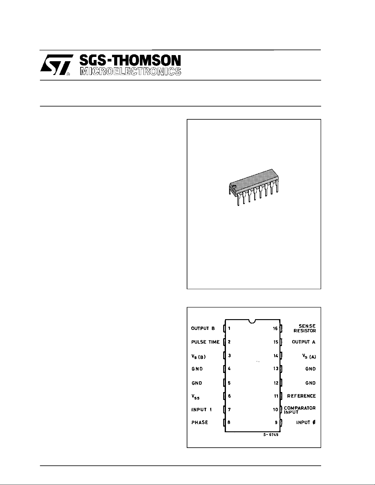
Powerdip 12 + 2 + 2
(PlasticPackage)
ORDER CODE : PBL3717A
DESCRIP TION
ThePBL3717AisamonolithicICwhichcontrolsand
drives one phase of a bipolar stepper motor with
choppercontrolofthe phasecurrent.Currentlevels
maybeselectedinthreestepsbymeansoftwologic
inputswhich select one of threecurrent comparators.Whenbothof theseinputsare highthe device
isdisabled.Aseparatelogicinputcontrolsthedirectionof current flow.
A monostable,programmedby an externalRC network,sets the currentdecaytime.
Thepower sectionisa full H-bridge driver with four
internal clamp diodes for current recirculation. An
externalconnectiontotheloweremittersisavailable
for the insertion of a sensing resistor. Two
PBL3717Asand few external componentsform a
completesteppermotor drive subsystem.
The raccomendedoperating ambient temperature
rangesis from 0 to 70 °C.
ThePBL3717Aissuppliedina12+2+ 2leadPowerdippackage.
April1993
PIN CONNECTI ON (top view)
1/11
PBL3717A
PIN FUNCTIONS
N° Name Function
1 UTPUT B Output Connection (with pin 15). The outputstage is a ”H” bridge formed by four
2 PULSE TIME A parallel RC network connected to this pin sets the OFF time of the lower power
3 SUPPLY VOLTAGE B Supply Voltage Input for Half Output Stage
4 GROUND Ground Connection. With pins 5, 12 and 13 also conducts heat from die to
5 GROUND See pin 4.
6 LOGIC SUPPLY Supply Voltage Input for Logic Circuitry
7 INPUT 1 This pin and pin 9 (INPUT 0) are logic inputs which select the outputs of the
8 PHASE This TTL-compatible logic input sets the directionof current flow through the
9 INPUT 0 See INPUT 1 (pin 7) .
10 COMPARATOR
INPUT
11 REFERENCE A voltage applied to this pin sets thereference voltage of the three comparators,
12 GROUND See pin 4.
13 GROUND See pin 4.
14 SUPPLY VOLTAGE A Supply Voltage Input for Half Output Stage. See also pin 13.
15 OUTPUT A See pin 1.
16 SENSE RESISTOR Connection to Lower Emitters of Output Stage for Insertion of Current Sense
transistors and four diodes suitable for switching applications.
transistors. The pulse generator is a monostable triggered by the rising edge of
the output of the comparators (t
= 0.69 RTCT).
off
See also pin 14.
printed circuit copper.
three comparators to set the current level. Current also depends on the sensing
resistor and reference voltage. See truth table.
load. A high level causes current to flow from OUTPUT A (source) to OUTPUT
B (sink). A schmitt trigger on this input provides good noise immunity and a delay
circuit prevents output stage short circuits during switching.
Input connected to the three comparators. The voltage across the sense resistor
is feedback to thisinput through the low pass filter R
transistor are disabled when the sense voltage exceeds the reference voltage of
. The lower power
CCC
the selected comparator. When this occursthe current decays for a time set by
R
TCT,toff
this determining the output current(also thus depending on R
INPUT 0 and INPUT 1).
= 0.69 RTCT.
and the two inputs
s
Resistor
TRUTH TABLE
Input 0 (pin 9) Input 1 (pin 7)
H
L
H
L
2/11
H
H
L
L
No Current
Low Current
Medium Current
High Current
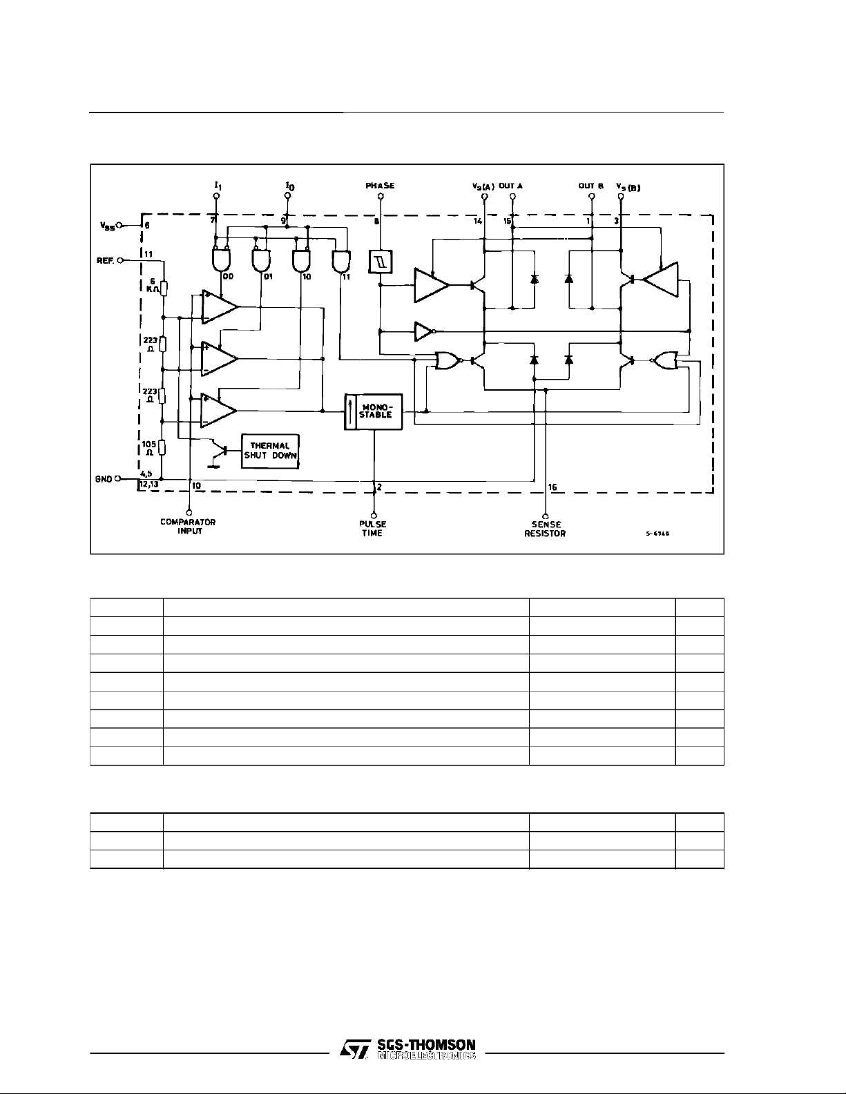
BLOCK DIAGRAM
PBL3717A
ABSOLUTE MAXIMUM RATINGS
Symbol Parameter Value Unit
V
s
V
ss
V
V
c
V
r
I
o
T
stg
T
j
Power Supply Voltage 50 V
Logic Supply Voltage 7 V
Logic Input Voltage 6 V
i
Comparator Input V
ss
Reference Input Voltage 15 V
Output Current (DC operation) 1.2 A
Storage Temperature – 55 to + 150 °C
Operating Junction Temperature 150 °C
THERMAL DATA
Symbol Parameter Value Unit
R
th j-case
R
th j-amb
*
Solderedon a 35µ thick 20cm
Thermal Resistance Junction-pins 11 °C/W
Thermal Resistance Junction-ambient* 40 °C/W
2
P.C.board copper area.
3/11
PBL3717A
ELECTRICAL CHARACTERISTICS
(refer to the test circuit V
= 36V, VSS= 5V, T
S
Symbol Parameter Test Conditions Min. Typ. Max. Unit
V
V
I
Supply Voltage (pin 3, 14) 10 46 V
s
Logic Supply Voltage (pin 6) 4.75 5.25 V
ss
Logic Supply Current (pin 6) 7 15 mA
ss
Reference InputCurrent (pin 11) VR= 5V 0.75 1 mA
I
R
LOGIC INPUTS
V
V
I
Input Low Voltage (pins 7, 8, 9) 0.8 V
iL
Input High Voltage (pin 7, 8, 9) 2 V
iH
Low Voltage Input Current (pins 7, 8, 9) Vi= 0.4V pin 8
I
iL
High Voltage Input Current (pins 7, 8, 9) Vi= 2.4V 10 µA
iH
COMPARATORS
V
V
V
t
I
Comparator Low Threshold Voltage (pin 10) VR=5V Io=L
CL
Comparator Medium Threshold Voltage (pin 10) VR=5V Io=L
CM
Comparator High Threshold Voltage (pin 10) VR=5V Io=L
CH
I
Comparator Input Current (pin 10) ± 20 µA
C
Cutoff Time RT= 56kΩ CT= 820pF 25 35 µs
off
Turn Off Delay (see fig. 2) 2 µs
t
d
Output Leakage Current (pins 1, 15) Io=H I1= H 100 µA
off
SOURCE DIODE-TRANSISTOR PAIR
V
V
I
I
V
SLK
Saturation Voltage (pins 1, 15) IM= – 0.5A (see fig. 2)
sat
Saturation Voltage (pins 1, 15) IM= – 1A (see fig. 2)
sat
Leakage Current Vs= 46 V 300 µA
LK
Diode Forward Voltage IM= – 0.5A
F
Substrate Leakage Current when Clamped IM= – 0.5A
SINK DIODE-TRANSISTOR PAIR
V
I
V
Saturation Voltage (pins 1, 15) IM= 0.5A
sat
Leakage Current Vs= 46V 300 µA
LK
Diode Forward Voltage IM= 0.5A
F
=25oC unless otherwise specified)
amb
pins 7, 9
=H
I
1
=H
I
1
=H
I
1
Conduction Period
Recirculation Period
Conduction Period
Recirculation Period
=–1A
I
M
=–1A
I
M
=1A
I
M
=1A
I
M
ss
– 100
– 400µAµA
66 78 90 mV
236 251 266 mV
396 416 436 mV
1.7
2.1
1.1
1.35
2.1
2.8
1.7
2.5
1
1.25
1.3
1.7
25mA
1.1
1.35
1.6
2.3
1.1
1.5
1.4
2
V
V
V
V
V
mA
V
V
V
V
4/11

Figure 1 : Test and ApplicationCircuit
Figure 2 : WaveformswithMA Regulating(phase= 0)
PBL3717A
5/11

PBL3717A
Figure 3 : TwoPhaseBipolarStepperMotor Driver
Figure 4 : P.C. Board and ComponentLayout of the Circuit of fig. 3 (1 : 1 scale)
6/11

Figure 5 : Inputand OutputSequencesfor Half Stepand FullStep Operation
PBL3717A
APPLIC ATI O N INFO RMATIO NS
Figure 3 shows a typical application in which two
PBL3717Acontrolatwo phasebipolarsteppermotor.
Programming
ThelogicinputsI
andI1setat threedifferentlevels
0
the amplitude of the current flowing in the motor
windingaccordingtothetruthtableofpage2.Ahigh
levelon the ”PHASE” logic input sets the direction
ofthatcurrentfromoutputA to outputB; a lowlevel
from outputB to outputA.
It is recommended that unused inputs are tied to
pin 6 (V
) or pin 4 (GND) as appropriateto avoid
ss
noiseproblem.
The current levels can be varied continuously by
changingthe ref.voltageon pin 11.
Control ofthe Motor
Thesteppermotorcanrotateineitherdirectionsaccording to the sequenceof the input signals. It is
possibletoobtaina fullstep, a half step anda quarter step operation.
Full StepOperation
Both the windings of the stepper motor are energizedall the time withthe same current I
I
andI1remainfixedat whatevertorquevalueisre-
0
MA=IMB
.
quired.
Calling A the conditionwith winding A energizedin
one direction and A in the other direction, the sequencefor fullstep rotation is :
AB → AB → AB → ABetc.
Forthe rotationin the otherdirection the sequence
must be reserved.
Inthefullstepoperationthetorqueisconstanteach
step.
HalfStep Operation
Power is applied alternately to one winding then
bothaccording to the sequence:
AB → B → AB → A → AB → B → AB → Aetc.
Likefull step thiscan be doneat anycurrentlevel;
the torqueis not constantbut it is lowerwhen only
one windingis energized.
A coilis turnedoff bysetting I
and I1bothhigh.
0
7/11

PBL3717A
QuarterStep Operation
It ispreferable to realizethe quarterstep operation
at full power otherwise the steps will be of very irregularsize.
Theextraquarterstepsare addedto the half steps
sequencebyputtingonecoilonhalf currentaccordingto the sequence.
A
AB →
B → B →
2
__
A
B→ AB → A
2
B
→ A etc.
2
MotorSelection
As the PBL3717Aprovides constantcurrent drive,
withaswitchingoperation,caremustbetakentoselect stepper motors with low hysteresis losses to
preventmotorover heat.
Figure6 : SourceSaturationVoltageversus
OutputCurrent (recircuitperiod)
L -C Filter
To reduce EMI and choppinglossesin themotora
lowpass L -C filter can be inserted acrossthe outputsofthePBL3717Aasshownonthefollowingpicture.
−10
L ≈
1
10
LM C ≈
⋅ 10
4
L
Figure7 : SourceSaturationVoltageversus
OutputCurrent(conductionperiod)
Figure8 : Sink SaturationVoltageversus
OutputCurrent
8/11
Figure9 : ComparatorThreshold versus
JunctionTemperature

PBL3717A
MOUNTINGINSTRUCTIONS
The R
of the PBL 3717A can be reduced by
th j-amb
solderingthe GNDpinsto asuitablecopperareaof
the printedcircuit board or to an external heatsink.
Figure10 : Exampleof P.C. BoardCopper Area
whichis usedas Heatsink
Thediagramoffig. 11showsthemaximumdissipable power P
andthe R
tot
as a functionof the
th j-amb
side”α” oftwo equal squarecopperareashaving a
thichknessof35µ (seefig. 10).
Figure11 : Max.Dissipable Power andJunction-
AmbientThermalResistanceversus
size ”a”
9/11

PBL3717A
POWERDIP16 PACKAGE MECHANICAL DATA
DIM.
MIN. TYP. MAX. MIN. TYP. MAX.
a1 0.51 0.020
B 0.85 1.40 0.033 0.055
b 0.50 0.020
b1 0.38 0.50 0.015 0.020
D 20.0 0.787
E 8.80 0.346
e 2.54 0.100
e3 17.78 0.700
F 7.10 0.280
I 5.10 0.201
L 3.30 0.130
Z 1.27 0.050
mm inch
10/11

PBL3717A
Information furnished is believed to be accurate and reliable. However, SGS-THOMSON Microelectronics assumes no responsibility for
the consequences of use of such information nor for any infringement of patents or other rights of third parties which may result from its
use. No license is granted by implication or otherwise under any patent or patent rights of SGS-THOMSON Microelectronics. Specifications mentioned in this publication are subject to change without notice. This publication supersedes and replaces all information previously supplied. SGS-THOMSON Microelectronics products are not authorized for use as critical components in life support devices or
systems withoutexpress written approval of SGS-THOMSON Microelectronics.
1994 SGS-THOMSON Microelectronics - All Rights Reserved
Australia - Brazil - France - Germany - Hong Kong - Italy - Japan - Korea - Malaysia - Malta - Morocco - The Netherlands - Singapore -
SGS-THOMSON Microelectronics GROUP OF COMPANIES
Spain - Sweden - Switzerland - Taiwan - Thaliand - UnitedKingdom - U.S.A.
11/11
 Loading...