


®
P01 Ser ies
SENSITIVE 0.8A SCRs
MAIN FEATURES:
Symbol Value Unit
I
T(RMS)
V
DRM/VRRM
I
GT
0.8 A
400 and 600 V
5 to 200 µA
DESCRIPTION
Thanks to highly sensitive triggering levels, the
P01 SCR series is suitable for all applications
where available gate current is limited, such as
ground fault circuit interruptors, pilot circuits in
solid state relays, stand-by mode power supplies,
smoke and alarm detectors.
Available in through-hole or surface mount packages, the voltage capability of this series has been
upgrated since its introduction, to reach 600 V.
TO-92
(P01xxA)
A
G
K
SOT-223
(P01xxN)
ABSOLUTE RATINGS (lim iting values)
Symbol Parameter Value Unit
I
T(RMS)
IT
(AV)
I
TSM
²
I
dI/dt
I
GM
P
G(AV)
T
stg
Tj
RMS on-state current
(180° conduction angle)
Average on-state current
(180° conduction angle)
Non repetitive surge peak on-state
current
tI
²
t Value for fusing
Critical rate of rise of on-state current
= 2 x IGT , tr ≤ 100 ns
I
G
Peak gate current tp = 20 µs Tj = 125°C 1 A
Average gate power dissipation Tj = 125°C 0.1 W
Storage junction temperature range
Operating junction temp erature range
September 2000 - Ed: 3
TO-92 Tl = 55°C
0.8 A
SOT-223 Tamb = 70°C
TO-92 Tl = 55°C
0.5 A
SOT-223 Tamb = 70°C
tp = 8.3 ms
tp = 10 ms 7
Tj = 25°C
8
tp = 10ms Tj = 25°C 0.24
F = 60 Hz Tj = 125°C 50 A/µs
- 40 to + 150
- 40 to + 125
A
2
S
A
°C
1/6
P01 Series
ELECTRICAL CHARACTERISTICS (Tj = 25°C, unless otherwise specified)
Symbol Test Conditions
P01xx
02 11 18
I
GT
VD = 12 V RL = 140 Ω
V
GT
V
V
dV/dt V
V
V
I
DRM
I
RRM
VD = V
GD
IRG = 10 µA
RG
I
I
H
I
L
TM
t0
R
= 50 mA RGK = 1 kΩ
T
IG = 1 mA RGK = 1 kΩ
= 67 % V
D
ITM = 1.6 A tp = 380 µs
Threshold voltage Tj = 125°C MAX. 0.95 V
Dynamic resistance Tj = 125°C MAX. 600 mΩ
d
V
DRM
V
DRM
V
DRM
RL = 3.3 kΩ RGK = 1 kΩ
DRM
RGK = 1 kΩ
DRM
= V
= V
= V
= 400 V RGK = 1 kΩ
RRM
= 600 V RGK = 1 kΩ
RRM
RGK = 1 kΩ
RRM
Tj = 125°C MIN.
Tj = 125°C MIN. 75 80 75 V/µs
Tj = 25°C MAX. 1.95 V
Tj = 25°C
Tj = 125°C MAX. 100 µA
MIN. - 4 0.5
MAX. 200 25 5
MAX. 0.8 V
0.1 V
MIN.
8V
MAX. 5 mA
MAX.
MAX.
6
1
10 µA
THERMAL RESISTANCES
Symbol Parameter Value Unit
R
th(j-i)
R
th(j-t)
th(j-a)
Junction to case (DC)
TO-92 80
Junction to tab (DC) SOT-223 30
Junction to ambient TO-92 150
S = 5 cm
²
SOT-223 60
Unit
µA
mA
µA
°C/W
°C/WR
S = Copper surface under tab
PRODUCT SELECTOR
Part Number
400 V 600 V
P0102DA X 200 µA TO-92
P0102DN X 200 µA SOT-223
P0102MA X 200 µA TO-92
P0102MN X 200 µA SOT-223
P0111DA X 25 µA TO-92
P0111DN X 25 µA SOT-223
P0111MA X 25 µA TO-92
P0111MN X 25 µA SOT-223
P0118DA X 5 µA TO-92
P0118DN X 5 µA SOT-223
P0118MA X 5 µA TO-92
P0118MN X 5 µA SOT-223
2/6
Voltage
Sensitivity
Package

P01 Series
µ
ORDERING INFORMATION
Blank
PACKAGE:
A:TO-92
N: SOT-223
PACKING MODE:
1AA3:TO-92 bulk (preferred)
2AL3:TO-92 ammopack
5AA4: SOT-223 Tape & Reel
SENSITIVE
SCR
SERIES
CURRENT:0.8A
P 01 02 D N 1AA3
VOLTAGE:
D: 400V
M: 600V
SENSITIVITY:
02: 200µA
11: 25µA
18: 5
A
OTHER INFORMATION
Part Number Marking Weight Base Quantity Packing mode
P01xxyA 1AA3 P01xxyA 0.2 g 2500 Bulk
P01xxyA 2AL3 P01xxyA 0.2 g 2000 Ammop ack
P0102yN 5AA4 P2y 0.12 g 1000 Tape & reel
P0111yN 5AA4 P1y 0.12 g 1000 Tape & reel
P0118yN 5AA4 P8y 0.12 g 1000 Tape & reel
Note: xx = sensitivity, y = voltage
Fig. 1: Maximum average power dissipation
versus average on-state current.
Fig. 2-1: Average and D.C. on-state current
versus lead temperature.
P(W)
1.0
0.9
0.8
0.7
0.6
0.5
0.4
0.3
0.2
0.1
0.0
0.0 0.1 0.2 0.3 0.4 0.5 0.6
Fig. 2-2: Average and D.C. on-state current
versus ambient temperature (device mounted o n
FR4 with recommended pad layout for SOT-223).
IT(av)(A)
1.2
1.1
1.0
0.9
0.8
0.7
0.6
0.5
0.4
0.3
0.2
0.1
0.0
02550
Tamb(°C)
75
100 125
IT(av)(A)
1.1
1.0
0.9
0.8
0.7
0.6
0.5
0.4
0.3
0.2
0.1
0.0
02550
Tlead orTtab (°C)
75
100 125
Fig. 3: Relative variation of thermal impedance
junction to ambient versus pulse duration.
K = [Zth(j-a)/Rth(j-a)]
1.00
0.10
0.01
1E-2 1E-1
1E+0
tp(s)
1E+1 1E+2
5E+2
3/6

P01 Series
Fig. 4: Relative variation of gate trigger current,
holding current and latching current versus
junction temperature (typical values).
IGT,IH, IL[Tj] / IGT,IH, IL[T] = 25°C
6
5
4
3
2
1
0
Tj(°C)
0-20-40 20 40 60 80 100 120 140
Fig. 6: Relative variation of dV/dt immunity
versus gate-cathode resistance (typical values).
dV/dt[Rgk] / dV/dt[Rgk=1k ]Ω
10.0
1.0
Fig. 5:Relative variation of holding current versus
gate-cathode resistance (typical values).
IH[Rgk]/IH[Rgk=1k ]Ω
Rgk(kΩ)
Fig. 7: Relative variation of dV/dt immunity
versus gate-cathode capacitance (typical values).
dV/dt[Cgk] / dV/dt[Rgk=1k ]Ω
10
8
6
4
Rgk(kΩ)
0.1
0
0.4 0.6 0.8 1.00.2 1.6 1.8 2.01.2 1.4
Fig. 8: Surge peak on-state current versus
number of cycles.
ITSM(A)
8
7
6
5
4
3
2
1
0
1 10 100 1000
Repetitive
Tamb=25°C
Non repetitive
Tj initial=25°C
tp=10ms
Onecycle
Numberofcycles
2
Cgk(nF)
0
03
21
5
4
6
7
Fig. 9: Non-repetitive surge peak on-state
current for a sinusoidal pulse with width
tp < 10 ms, and corresponding value of I²t.
ITSM(A), I t(A s)
100.0
10.0
1.0
0.1
0.01
22
0.10
tp(ms)
1.00
10.00
4/6
P01 Series
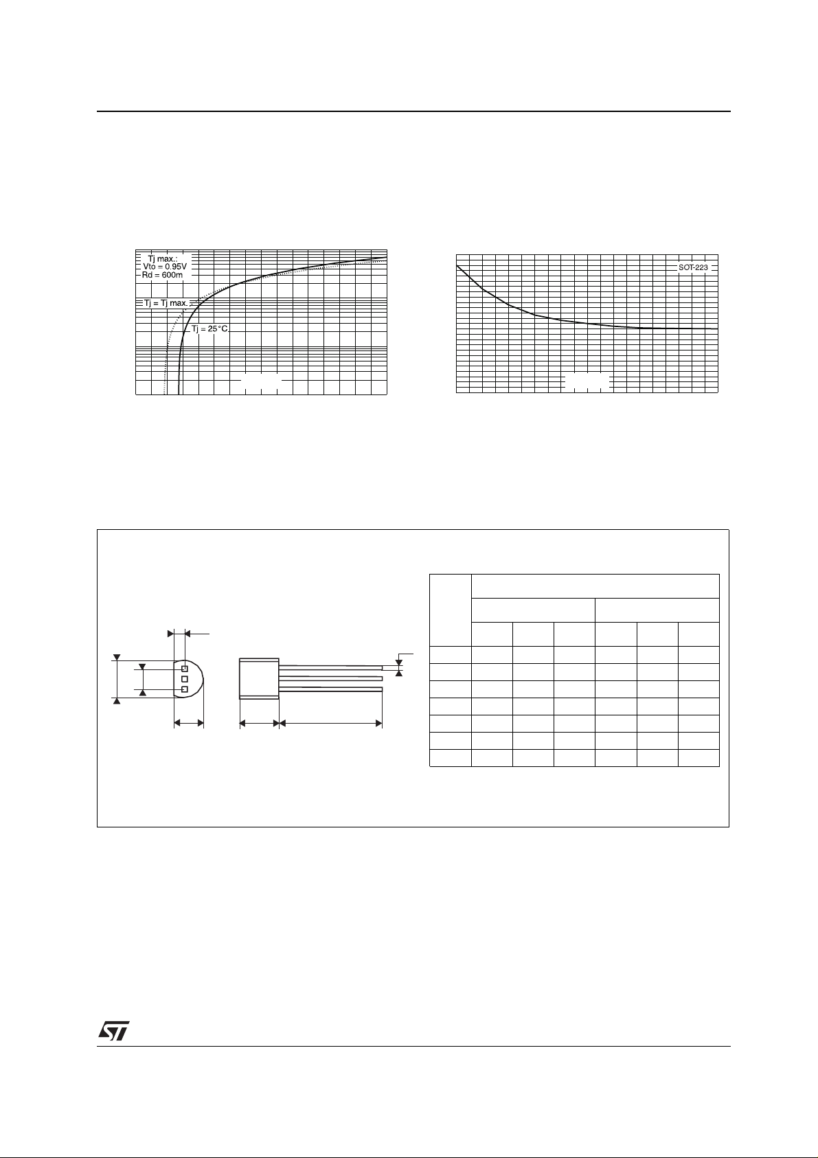
Fig. 10: On-state characteristics (maximum
values).
ITM(A)
1E+1
Ω
1E+0
1E-1
1E-2
0.5 1.0 1.5 2.0 2.5 3.0 3.5 4.0 4.5
VTM(V)
PACKAGE MECHANICAL DATA
TO-92 (Plastic)
Fig. 11: SOT-223 Therm al resistance junction to
ambient versus copper surface under tab (Epoxy
printed circuit board FR4, copper thickness:
35 µm).
Rth(j-a) (°C/W)
130
120
110
100
90
80
70
60
50
40
30
20
10
0
0.0 0.5 1.0 1.5 2.0 2.5 3.0 3.5 4.0 4.5 5.0
S (cm )
2
BAC
DIMENSIONS
REF.
Millimeters Inches
Min. Typ. Max. Min. Typ. Max.
a
A 1.35 0.053
B 4.70 0.185
C 2.54 0.100
D 4.40 0.173
F
D
E
E 12.70 0.500
F 3.70 0.146
a 0.50 0.019
5/6

P01 Series
PACKAGE MECHANICAL DATA
SOT-223 (Plastic)
A
A1
B
e1
D
B1
H
E
e
V
DIMENSIONS
c
REF.
Millimeters Inches
Min. Typ. Max. Min. Typ. Max.
A 1.80 0.071
A1 0.02 0.1 0.0008 0.004
B 0.60 0.70 0.85 0.024 0.027 0.034
B1 2.90 3.00 3.15 0.114 0.118 0.124
c 0.24 0.26 0.35 0.009 0.010 0.014
D 6.30 6.50 6.70 0.248 0.256 0.264
e 2.3 0.090
e1 4.6 0.181
E 3.30 3.50 3.70 0.130 0.138 0.146
H 6.70 7.00 7.30 0.264 0.276 0.287
V 10° max
FOOTPRINT DIMENSIONS (in millimete r s )
SOT-223 (Plastic)
Information furnished is believed to be accurate and reliable. However, STMicroelectronics assumes no responsibility for the consequences
of use of su ch in for mat i on n or f or a ny in fr ing em ent of pa te nts or o ther r igh ts of th ir d pa r tie s w hic h may res ul t f rom i ts us e. No license is granted
by impl i cation or ot herwise under any patent or patent r i ght s of STMi croelectro ni cs. Specif i cations mentioned i n this publ i cation are subje ct
to change wi t hout notice. T hi s publicati on supersede s and replaces all in formation previously supplied. STM i croelectro ni cs products are not
authori zed for use as cr i tical compo nents in life support devices or systems without ex press written approva l o f ST M i croelectr o nics.
© The ST logo is a registered trademark of STMicroelectronics
6/6
© 2000 STMicroelectronics - Printed in Italy - All Rights Reserved
STMicroele ct ronics GROUP OF COM PANIES
Australi a - Brazil - Chi na - Finlan d - F rance - Germ any - Hong Kon g - India - Italy - Japan - Ma l aysia - Malta - Morocco
Singapo re - Spain - Sweden - Swit zerland - Un i ted Kingdom
http://w ww.st.com
 Loading...