

SGS Thomson Microelectronics MSC82040 Datasheet
RF & MICROWAVE TRANSISTORS
.EMITTER BALLASTED
.CLASS A LINEAR OPERATION
.COMMON EMITTER
.VSWR CAPABILITY
CONDITIONS
:1 @ RATED
∞
.ft 1.6 GHz TYPICAL
.NOISE FIGURE 15.5 dB @ 2 GHz
.P
= 27 dBm MIN. @ 1.0 GHz
OUT
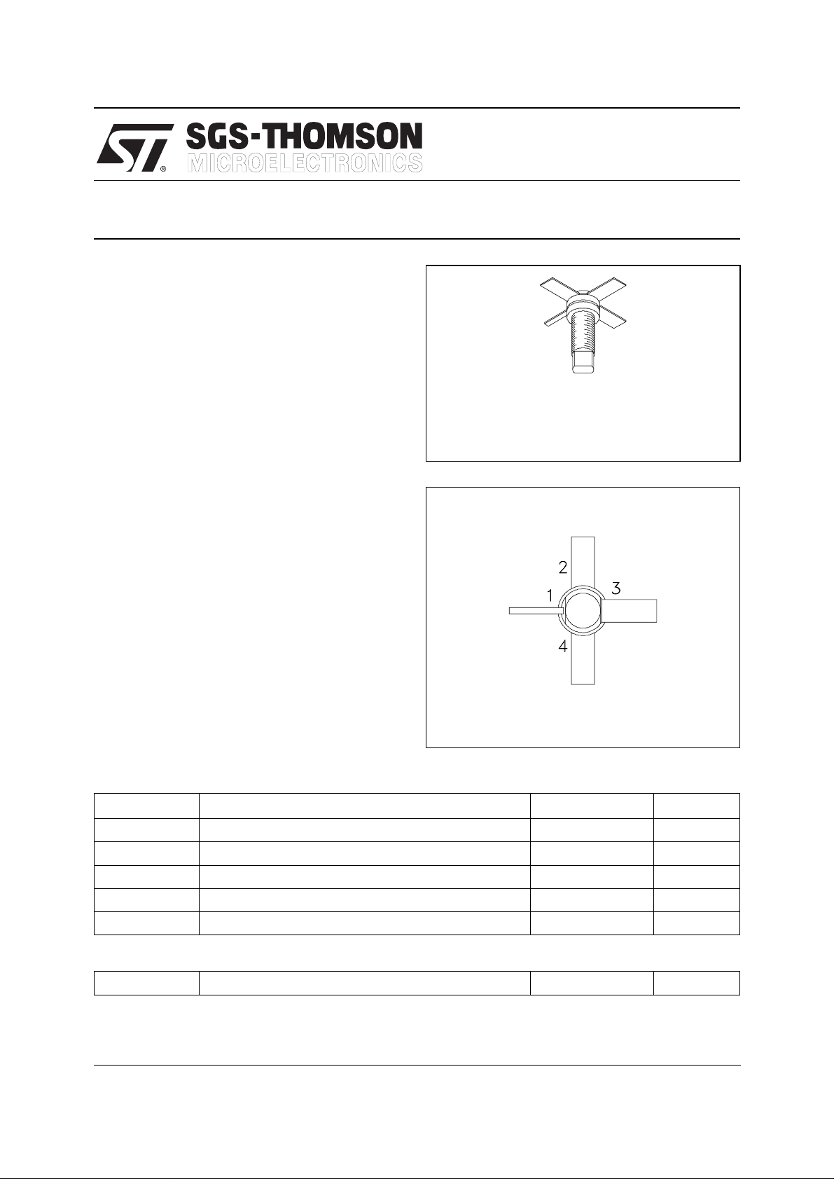
.230 4L STUD (S027)
ORDER CO DE
MSC82040
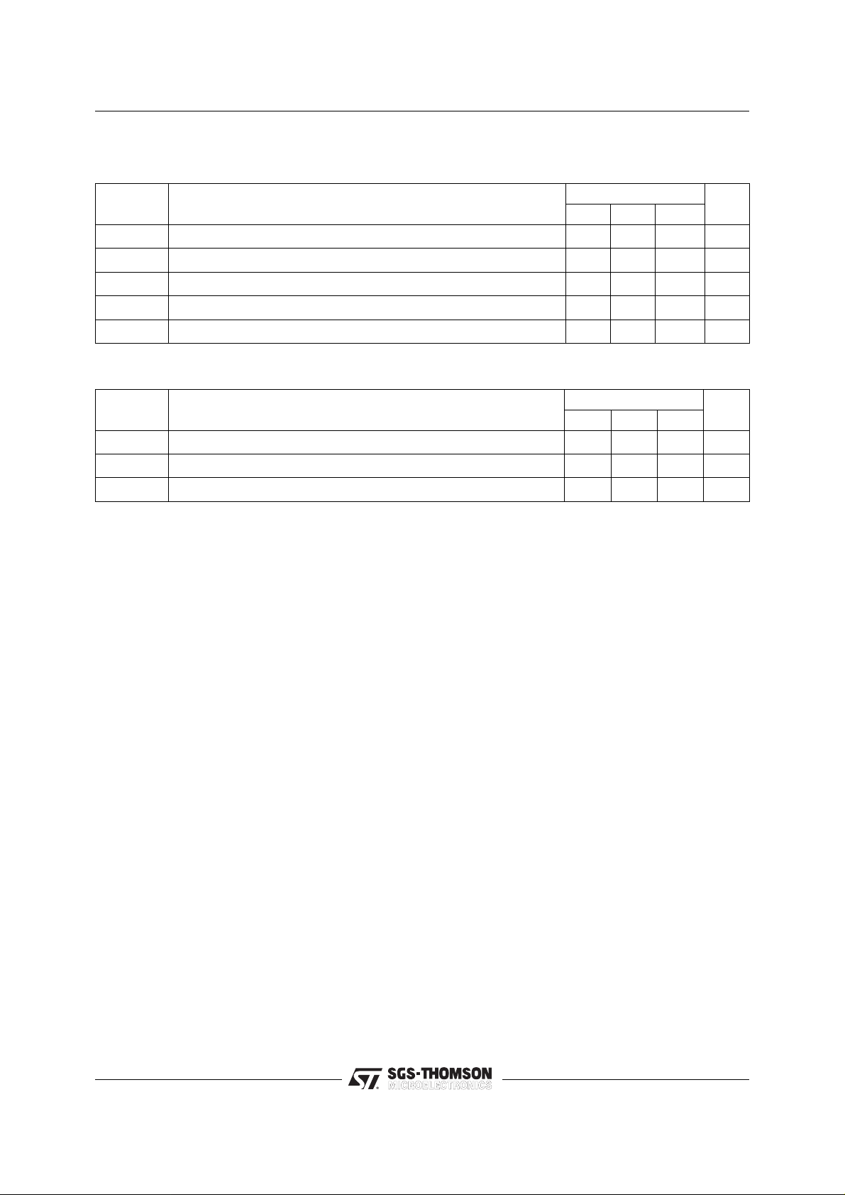
PIN CONNECTION
MSC82040
GENERAL PURPOSE LINEAR APPLICATIONS
hermetical ly sealed
BRANDING
82040
DESCRIPTION
The MSC82040 is a hermetically sealed NPN
power transistor with a fishbone, emitter finger
ballasted geometry utilizing a refractory/gold metallization system. The device is designed specifically for Class A linear applications to provide
high gain and high output power at the 1.0 dB
compression point.
ABSOLUTE MAXIMUM RATINGS (T
Symbol Parameter Value Unit
P
DISS
I
C
V
CE
T
J
T
STG
THERMAL DATA
R
TH(j-c)
*Applies only to rated RF amplifier operation
Power Dissipation (see Safe Area) — W
Device Bias Current 200 mA
Collector-Emitter Bias Voltage* 20 V
Junction Temperature 200
Storage Temperature
Junction-Case Thermal Resistance* 20
case
= 25°C)
1. Collector 3. Base
2. Emitter 4. Emitter
65 to +200
−
°
°
°
C/W
C
C
October 1992
1/6
MSC82040
ELECTRICAL SPECIFICATIONS (T
case
= 25°C)
STATIC
Symbol Test Condition s
BV
BV
BV
I
CBO
EBO
CEO
CEO
h
FE
IC = 1mA IE = 0mA 45 — — V
IE = 1mA IC = 0mA 3.5 — — V
IC = 5mA IB = 0mA 20 — — V
VCE = 18V — — 0. 5 mA
VCE = 5V IC = 100mA 15 — 120 —
DYNAMIC
Symbol Test Conditions
GP*f = 1.0 GHz P
∆GP*f = 1.0 GHz P
C
OB
* Note: VCE = 18V
f = 1 MHz VCB = 28 V — — 3.2 pF
IC
100mA
=
= 27 dBm 10.5 11.5 — dB
OUT
27 dBm
=
OUT
Valu e
Min. Typ. Max.
Value
Min. Typ. Max.
P
= 10 dB — — 1 d B
∆
OUT
Unit
Unit
2/6
 Loading...