

SGS Thomson Microelectronics MSC81325M Datasheet
RF & MICROWAVE TRANSISTORS
.REFRACTORY/GOLD METALLIZATION
.EMITTER BALLASTED
.RUGGEDIZED VSWR
∞
:1
.INPUT/OUTPUT MATCHING
.OVERLAY GEOMETRY
.METAL/CERAMIC HERMETIC PACKAGE
.P
DESCRIPTION
The MSC81325M device is a high power pulsed
transistor specifically designed for DME/TACAN
avionics applications.
This device is capable of withstanding an infinite
load VSWR at any phase angle under full rated
conditions. Low RF thermal resistance and semiautomatic bonding techniques ensure high reliability and product consistency.
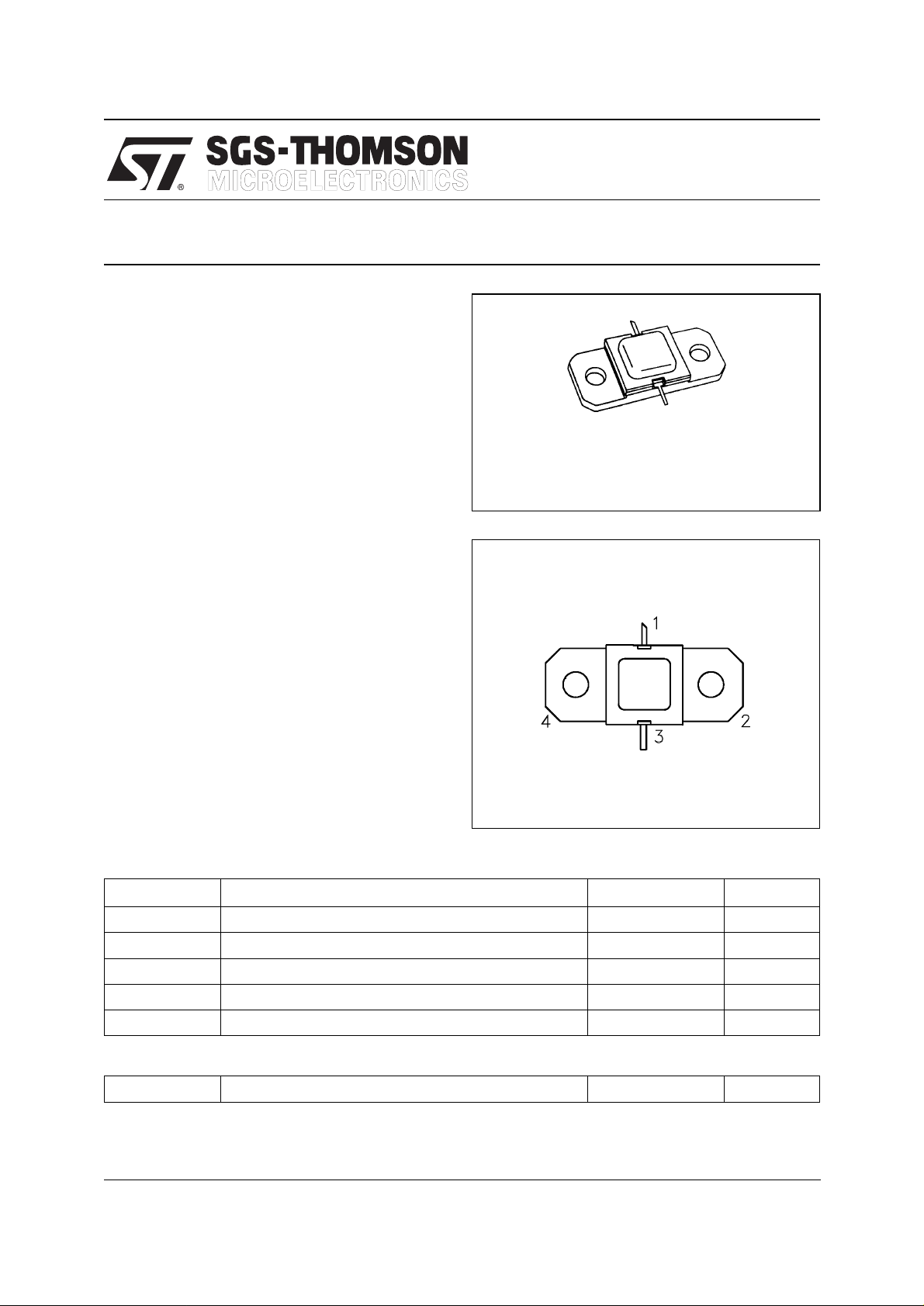
The MSC81325M is housed in the industry-standard AMPAC™ metal/ceramic hermetic package
with internal input/output matching structures.
= 325 W MIN. WITH 6.7 dB GAIN
OUT
.400 x .400 2NLFL (S 042)
ORDER CO DE
MSC81325M
PIN CONNECTION
1. Collector 3. Emitter
2. Base 4. Base
MSC81325M
AVIONICS APPLICATIONS
PRELIMINARY DATA
hermetical ly sealed
BRANDING
81325M
ABSOLUTE MAXIMUM RATINGS (T
Symbol Parameter Value Unit
P
DISS
I
C
V
CC
T
J
T
STG
THERMAL DATA
R
TH(j-c)
*Applies only to rated RF amplifier operation
October 1992
Power Dissipation* (TC ≤ 100˚C) 880 W
Device Current* 24 A
Collector-Supply Voltage* 55 V
Junction Temperature (Pulsed RF Operation) 250
Storage Temperature
Junction-Case Thermal Resistance* 0.17
case
= 25°C)
65 to +200
−
°
°
°
C/W
C
C
1/3
MSC81325M
ELECTRICAL SPECIFICATIONS (T
case
= 25°C)
STATIC
Symbol Test Condi tions
BV
BV
BV
I
CBO
EBO
CER
CES
h
FE
IC = 10mA IE = 0mA 65 — — V
IE = 1mA IC = 0mA 3.5 — — V
IC = 25mA RBE = 10Ω 65 — — V
VBE = 0V VCE = 50V — — 25 mA
VCE = 5V IC = 1A 15 — 120 —
Min. Typ. Max.
Valu e
DYNAMIC
Symbol Test Conditi ons
P
OUT
η
cf = 1025 — 1150 MHz PIN = 70 W VCC = 50 V 40 41 — %
G
P
Note: Pulse Widt h=10µSec
f = 1025 — 1150 MHz PIN = 70 W VCC = 50 V 325 360 — W
f = 1025 — 1150 MHz PIN = 70 W VCC = 50 V 6.7 7.1 — dB
Duty Cycle=1%
Value
Min. Typ. Max.
Unit
Unit
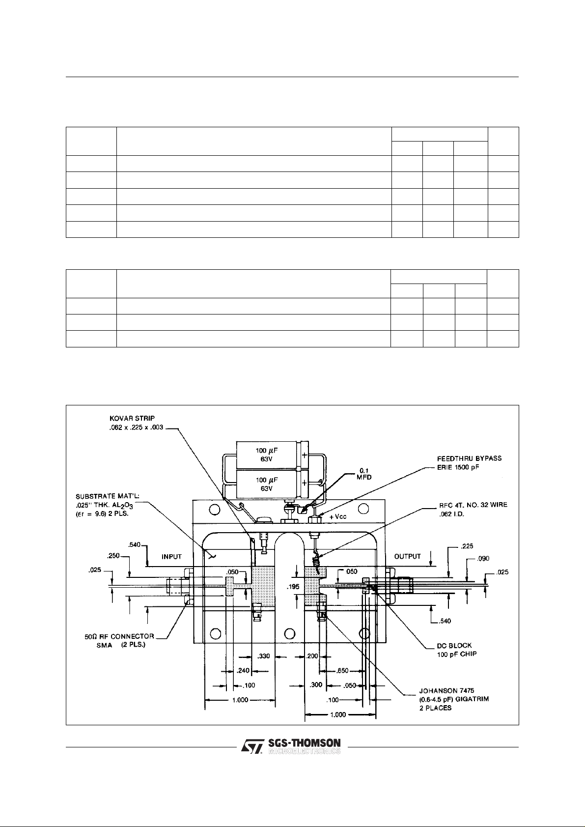
TEST CIRCUIT
All dimensions are in inches.
Ref.: Dwg. No. C127471
2/3
 Loading...