

SGS Thomson Microelectronics MK68901 Datasheet
.8 INPUT/OUTPUTPINS
• Individually programmable direction
• Individualinterrupt source capability
Programmable edge selection
-
.16 SOURCEINTERRUPTCONTROLLER
• 8 Internal sources
• 8 External sources
• Individualsource enable
• Individualsource masking
• Programmable interrupt service modes
Polling
-
Vectorgeneration
-
OptionalIn-service status
-
• Daisychaining capability
.FOUR TIMERS WITH INDIVIDUALLY PRO-
GRAMMABLE PRESCALING
• Twomultimode timers
Delaymode
-
Pulse width measurement mode
-
Event countermode
-
• Twodelay mode timers
• Independent clockinput
• Timeout output option
.SINGLECHANNEL USART
• Full Duplex
• Asynchronous to 65kbps
• Bytesynchronous to 1 Mbps
• Internal/External baud rate generation
• DMAhandshake signals
• Modemcontrol
• Loop back mode
.68000BUS COMPATIBLE
.48 PIN DIP OR 52 PIN PLCC
MK68901
MULTI–FUNCTION PERIPHERAL
1
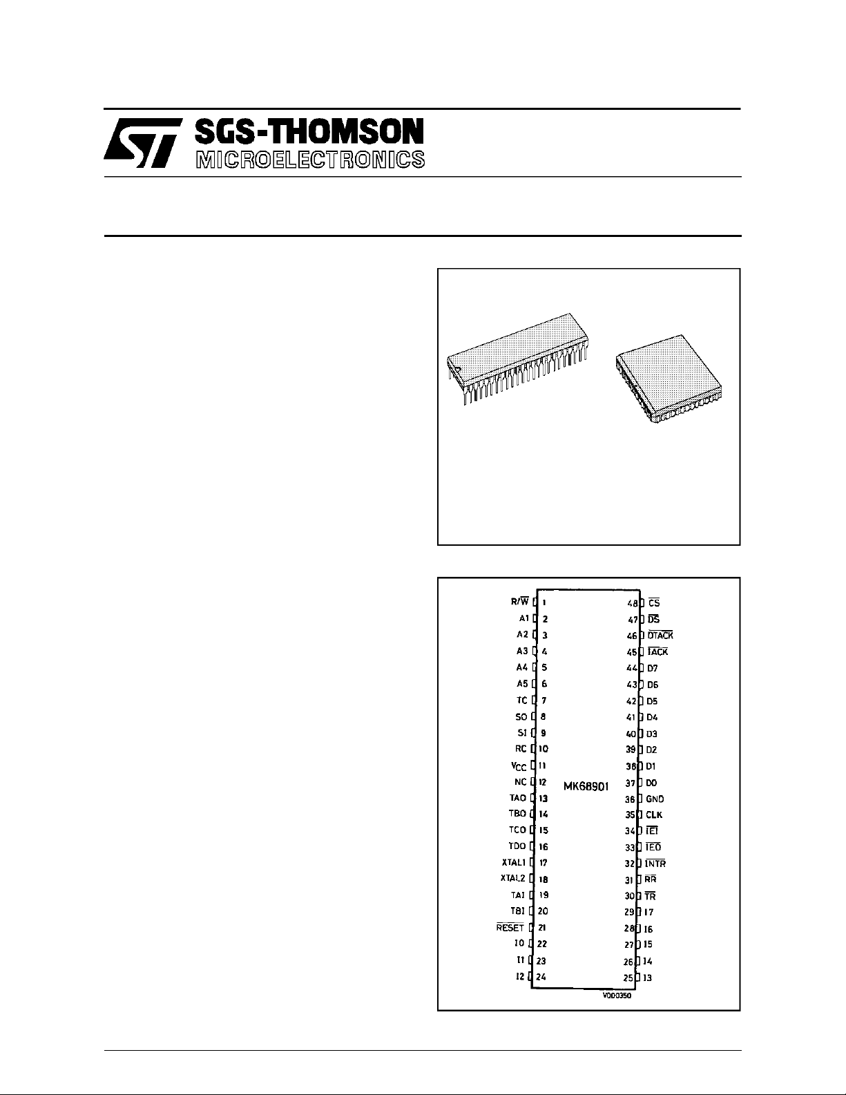
DPIP48 PLCC52
Figure1 : Pin connections.
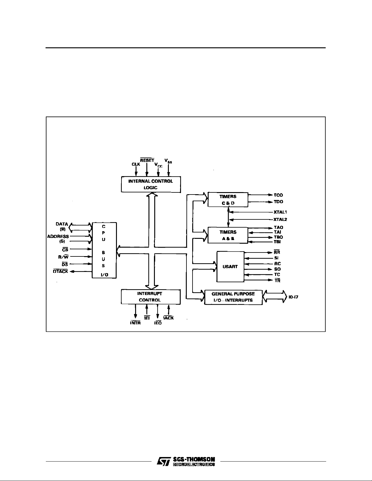
DESCRI PT ION
The MK68901 MFP (Multi-Function Peripheral) is a
combination of many of the necessary peripheral
functions in a microprocessor system.
Included are :
Eight parallel I/O lines
Interrrupt controller for 16 sources
Four timers
Single channelfull duplex USART
The useof the MFPin a system cansignificantly reducechipcount,thereby reducing systemcost. The
MFPiscompletely 68000buscompatible,and24directlyaddressable internal registers providethe ne-
December1988
MFP
1/33

MK68901
necessary control and status interface to the programmer.
The MFP is a derivative of the MK3801 STI, a Z80
familyperipheral.
PIN DESCRIPTION
GND : Ground
VCC: +5 volts (± 5%)
CS : Chip Select (input, active, low). CS is u-
sed toselect the MK68901 MFP for accessesto the internal registers. CS and
IACK must not be asserted at the same
time.
DS : Data Strobe (input, active low). DS is u-
sedaspartofthechipselectandinterrupt
acknowledge functions.
R/W : Read/Write (input). R/W is the signal
from the bus master indicating whether
thecurrent bus cycle is a Read (High) or
Write (Low) cycle.
DTACK: DataTransfer Acknowledge. (output,ac-
tive low, tri-stateable) DTACK is used to
signalthebus master that data is ready,
or that data has been accepted by the
MK68901 MFP.
A1-A5 : Address Bus (inputs).The adress bus is
used to adress one of the internal registersduring a read or write cycle.
D0-D7 : Data Bus (bi-directional, tri-stateable).
Thedatabusisusedtoreceive datafrom
or transmit data to one of the internal registers during a read or write cycle. It is
also used to pass a vector during an interruptacknowledge cycle.
CLK : Clock (input). This input is used to pro-
vide the internal timing for theMK68901
MFP.
RESET: Device reset. (input, active low). Reset
disablesthe USART receiver and transmitter,stops all timers and forcesthe timer outputs low, disables all interrupt
channels and clears any pending interrupts.The General PurposeInterrupt/I/O
lines will be placed in the tri-state input
mode.Allinternal registers (except the timer,USART dataregisters, and transmit
status register) will be cleared.
INTR : Interrupt Request (output, active low, o-
pen drain). INTR is asserted when the
MK68901 MFP isrequesting aninterrupt.
INTR is negated during an interrupt ac-
knowledge cycle or by clearing the pending interrupt(s) throughsoftware.
IACK: Interrupt Acknowledge (input, active
low).IACKisusedtosignaltheMK68901
MFP that the CPU is acknowledging an
interrupt. CS and IACk must not be assertedat the same time.
IEI : Interrupt Enable In (input,active low). IEI
is used to signal the MK68901 MFP that
no higherpriority device is requesting interrupt service.
IEO : InterruptEnable Out (output, active low).
IEO is used to signal lower priority peripherals that neither the MK68901 MFP
nor another higher priority peripheral is
requesting interrupt service.
10-17 : General Purpose Interrupt I/O lines.
Theselines may be used as interrupt inputs and/or I/O lines. When used as interrupt inputs, their active edge is programmable. A datadirection registerisused to define which lines are to be Hi-Z
inputsand whichlinesareto bepush-pull
TTL compatible outputs.
SO: SerialOutput.This is the outputof the U-
SART transmitter.
SI : Serial Input. This is the input to the U-
SART receiver.
RC : Receiver Clock. This input controls the
serialbit rate of theUSART receiver.
TC : TransmitterClock.Thisinput controlsthe
serialbit rate of theUSART transmitter.
RR : Receiver Ready. (output, active low)
DMA output for receiver, which reflects
the status of Buffer Full in port number
15.
TR : Transmitter Ready. (output, active low)
DMA output for transmitter, which reflects the status of Buffer Empty in port
number 16.
TAO,TBO,
TCO,TDO:
XTAL1,
XTAL2 :
Timer Outputs. Each of the four timers
has an output which can produce a
square wave. The output will change
stateseach timercycle ; thusone fullperiod of thetimer out signal is equalto two
timer cycles. TAO or TBO can be reset
(logic”O”) by a write to TACR, or TBCR
respectively.
Timer Clock inputs. A crystal can be
connected between XTAL1 and XTAL2,
or XTAL1 can be driven with a TTL level
clock.Whendriving XTAL1 withaTTL le-
2/33
MK68901
velclock,XTAL2mustbe allowedtofloat.
Whenusingacrystal,externalcapacitors
are required. See figure 33. All chip accesses are independent of the timer
clock.
TAI,TBI: TimerA,Binputs. Usedwhenrunning the
timers in the event count or the pulse
width measurement mode. The interrupt
channelsassociated with 14 and 13 are
usedforTAIandTBI,respectively.Thus,
when running a timer in the pulse width
V000351
3/33

MK68901
Figure 4 : RegisterMap.
Address Port N °. Abbreviation Regi ster Name
0
1
2
3
4
5
6
7
8
9
A
B
C
D
E
F
10
11
12
13
14
15
16
17
GPIP
AER
DDR
IERA
IERB
IPRA
IPRB
ISRA
ISRB
IMRA
IMRB
VR
TACR
TBCR
TCDCR
TADR
TBDR
TCDR
TDDR
SCR
UCR
RSR
TSR
UDR
GENERAL PURPOSE I/O
ACTIVE EDGE REGISTER
DATA DIRECTION REGISTER
INTERRUPT ENABLE REGISTER A
INTERRUPT ENABLE REGISTER B
INTERRUPT PENDING REGISTER A
INTERRUPT PENDING REGISTER B
INTERRUPT IN-SERVICE REGISTER A
INTERRUPT IN-SERVICE REGISTER B
INTERRUPT MASK REGISTER A
INTERRUPT MASK REGISTER B
VECTOR REGISTER
TIMER A CONTROL REGISTER
TIMER B CONTROL REGISTER
TIMERS C AND D CONTROL REGISTER
TIMER A DATA REGISTER
TIMER B DATA REGISTER
TIMER C DATA REGISTER
TIMER D DATA REGISTER
SYNC CHARACTER REGISTER
USART CONTROL REGISTER
RECEIVER STATUS REGISTER
TRANSMITTER STATUS REGISTER
USART DATA REGISTER
IN TERRUP TS
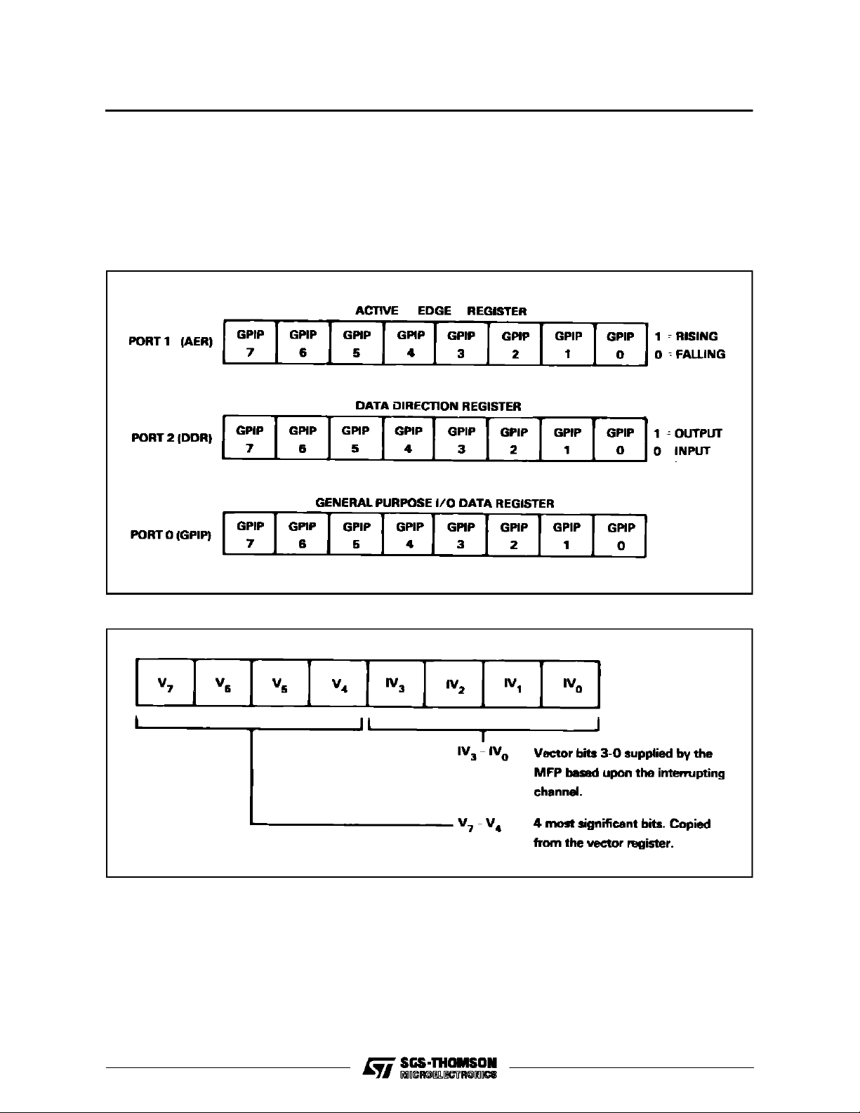
The GeneralPurpose I/O-InterruptPort(GPIP) provides eight I/O lines that may be operated eitheras
inputsor outputsundersoftwarecontrol. In addition,
each line may generate an interrupt in either a positivegoing edge or a negative goingedge ofthe input signal.
The GPIP has three associated registers. One allows the programmer to specify the ActiveEdgefor
eachbitthatwilltrigger an interrupt. Another register
specifies the Data Direction (input or output) associated with each bit. The thirdregister is the actual
data I/O register used to input or output datato the
port. These three registers are illstrated in figure5.
The ActiveEdge Register (AER) allows each of the
General Purpose Interrupts to provide an interrupt
on either a 1-0 transition or a 0-1 transition. Writing
a zero to the appropriate bit of the AER causes the
associatedinput to produce an interrupt on the 1-0
transition. The edgebit is simply one input to an exclusive-orgate, withthe otherinput comingfrom the
input buffer ant the output going to a 1-0 transition
detector. Thus, depending upon the state of the input, writing the AER can cause an interrupt-producing transition,which will cause an interrupt on the
associatedchannel, if that channel is enabled. One
would then normally configure the AER before
enabling interrupts via IERA and IERB.
Note : Changing the edge bit, with the interrupt
enabled, may cause an interrupt on that channel.
TheDataDirection Register(DDR)isusedtodefine
10-17 as inputs or as outputs on a bit by bit basis.
Writinga zero into a bit of the DDR causes the corresponding Interrupt-I/O pin to be a Hi-Z input. Writing a one into a bit of the DDR causes the corresponding pin to be configured as a push-pull output. When data is written into the GPIP,those pins
definedas inputs willremainin theHi-Z state while
those pins definedas outputs will assume the state
(high or low) of their corresponding bit in the GPIP.
When the GPIP is read, the data readwill come directlyfromthecorresponding bitoftheGPIPregister
forallpinsdefinedas output, whilethe data read on
all pins defined as inputs will come from the input
buffers.
Eachindividual functionin the MK68901isprovided
withauniqueinterruptvectorthatispresentedtothe
systemduring the interrupt acknowledgecycle.The
interrupt vector returned during the interrupt acknowledge cycleis shownin figure 6,whilethe vectorregisteris shown in figure7.
4/33
MK68901
There are 16 vectoraddresses generated internally
by the MK68901, one for each of the 16 interrupt
channels.
The Interrupt Control Registers (figure 8) provide
controlof interrupt processing for all I/O facilitiesof
the MK68901. These registers allow the program-
Figure 5 : General Purpose I/O Registers.
mer to enable or disable any or all of the 16 interrupts,providing maskingfor any interrupt, and provide accessto the pending and in-service status of
the interrupt. Optional end-of-interrupt modes are
available under software control. All the interrupts
areprioritized as shown in figure 9.
Figure 6 : Interrupt Vector.
V000352
V000353
5/33
MK68901
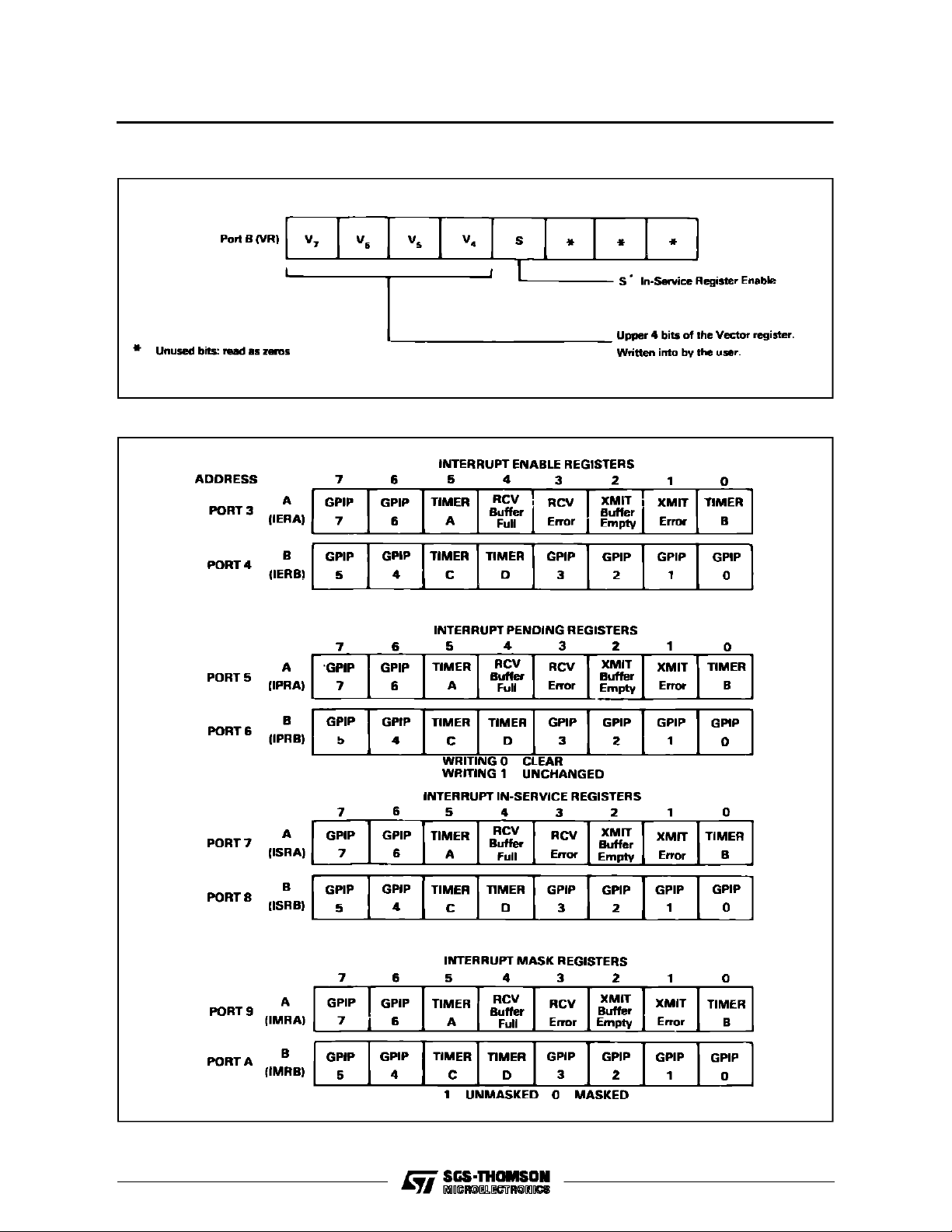
Figure 7 : VectorRegister.
Figure 8 : InterruptControl Registers.
V000354
6/33
V000355

Figure 9 : Interrupt Control Register Definitions
Priority Channel Descriptio n
HIGHEST
LOWEST
1111
1110
1101
1100
1011
1010
1001
1000
0111
0110
0101
0100
0011
0010
0001
0000
General Purpose Interrupt 7(I7)
General Purpose Interrupt 6(I6)
Timer A
Receive Buffer Full
Receive Error
Transmit Buffer Empty
Transmit Error
Timer B
General Purpose Interrupt 5(I5)
General Purpose Interrupt 4(I4)
Timer C
Timer D
General Purpose Interrupt 3(I3)
General Purpose Interrupt 2(I2)
General Purpose Interrupt 1(I1)
General Purpose Interrupt 0(I0)
MK68901
Interrupts may be either polled or vectored. Each
channel may be individual enabled or disabled by
writinga one or a zeroin theappropriate bitof Interrupt EnableRegisters (IERA, IERB-seefigure 8for
all registers in this section). When disabled, an interrupt channel is completely inactive. Any internal
or externalaction which would normally produce an
interrupt onthatchannelis ignored and anypending
interrupt onthat channel willbecleared by disabling
that channel.Disabling aninterrupt channel hasno
effect on the corresponding bit in Interrupt In-Service Registers (ISRA, ISRB); thus,if the In-service
Registersare used and an interrupt is in service on
that channelwhenthe channel is disabled, itwillremain in service until cleared in the normal manner.
IERA and IERB are alsoreadable.
When an interrupt is received on an enabled channel, itscorresponding bit in the pending register will
be set. When that channel is acknowledged it will
pass its vector,and thecorresponding bit in the Interrupt Pending Register (IPRA or IRPB) will be
cleared. IPRA and IPRBare readable ; thus by polling IPRA and IPRB, it can be determined whether
a channel has a pending interrupt. IPRA and IPRB
are also writeable and a pending interrupt can be
clearedwithout goingthrough the acknowledge sequence by writing a zero to the appropriate bit.This
allowsanyonebitto becleared, without alteringany
other bits, simply by writing all ones exceptfor the
bit position to be cleared to IPRA or IPRB. Thus a
fully polled interrupt schemeis possible. Note : writing a one to IPRA,IPRB has no effect on the interrupt pending register.
The interrupt maskregisters (IMRAand IMRB)may
beused to blocka channelfrommakingan interrupt
request. Writinga zero intothe corresponding bit of
the mask register will still allow the channel to receive an interrupt and latch it into its pending bit (if
thatchannel is enabled), but willprevent that channelfrom makingan interrupt request. Ifthat channel
is causing an interrupt request at the time the corresponding bit inthe maskregister iscleared, therequest willcease.If no other channel is making a request, INTRwillgo inactive. If the mask bitis re-enabled, any pending interrupt is now free to resume
its request unless blocked by a higher priority requestforservice. IMRAand IMRBarealsoreadable
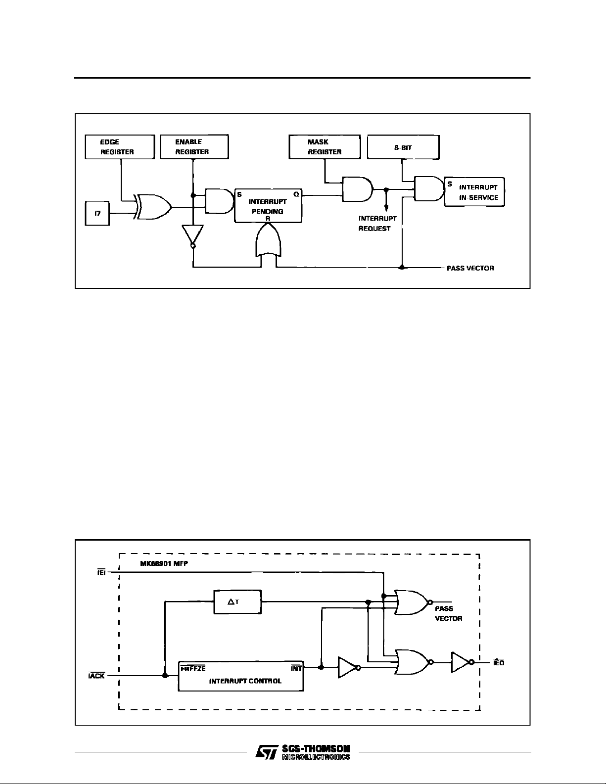
. A conceptual circuit of an interrupt channel is
shownin figure10.
7/33
MK68901
Figure 10 : A Conceptual Circuitof an Interrupt Channel.
V000356
Therearetwoend-of-interrupt modes : the automatic end-of-interrupt mode andthesoftwareend-of-interruptmode. Themodeisselected by writinga one
or a zero to the S bit of theVector Register (VR). If
the S bit of the VR is a one, all channels operate in
the software end-of-interrupt mode. If the S bitis a
zero, all channels operate in the automatic end-ofinterrupt mode, and a reset is held on all in-service
bits. In the automatic end-of-interrupt mode, the
pending bit is cleared when that channel passes its
vector. At that point, no further history of that interrupt remains in the MK68901 MFP. In the software
end-of-interrupt mode, the in-service bit is set and
the pending bit is cleared when the channel passes
itsvector.Withthein-service bitset,nolowerpriority
channelisallowed torequest an interrupt or topass
its vector during an acknowledge sequence ; however, a lower priority channelmaystillreceive an interruptand latchit intothepending bit.Ahigher priority channelmay stillrequestan interrupt andbe ac-
knowledged. The in-service bitof a particularchannel may be cleared by writing a zero to the corresponding bit in ISRA or ISRB. Typically, thiswill be
done at the conclusion of the interrupt routine just
before thereturn. Thusno lower priority channelwill
beallowedto requestserviceuntil thehigherpriority
channel is complete, while channels of still higher
priority will be allowed torequest service. While the
in-service bit isset,a secondinterrupt on that channelmaybereceivedandlatched intothependingbit,
though no service request will be made in response tothesecond interrupt untilthein-service bit
iscleared. ISRA and ISRB mayberead atany time.
Only a zero may be writtenintoany bit of ISRA and
ISRB;thusthein-servicebitsmaybe cleared insoftwarebut cannotbe set insoftware.This allows any
onebit tobe cleared, without alteringany other bits,
simplyby writingall ones except for the bit position
to be cleared to ISRA or ISRB, as with IPRA and
IPRB.
Figure 11 a : A Conceptual Circuit of the MK68901 MFP Daisy Chaining.
8/33
V000357
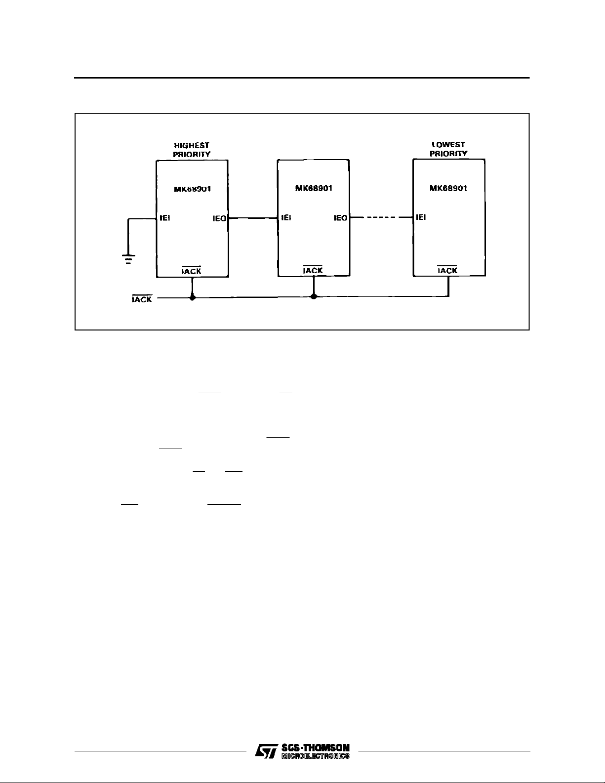
Figure 11 b : Daisy Chaining.
MK68901
V000358
Each interrupt channel respondswith a discrete 8bit vector when acknowledged. The upper four bits
of the vector are setby writing the upper four bits of
the VR.The four low order bits (bit 3-bit 0) are generatedby the interrupting channel.
Toacknowledge aninterrupt, IACKgoeslow,theIEI
inputmustgolow (or be tiedlow)and the MK68901
MFPmust have an acknowledgeable interrupt pending. The Daisy Chaining capability (figure 11) requires that allpartsin achainhaveacommonIACK.
Whenthe common IACK goes low, all parts freeze
and prioritize interrupts in parallel. Then priority is
passeddownthe chain, via IEI and IEO, untila part
which has a pending interrupt is reached. The part
withthepending interrupt, passesa vector,doesnot
propagate IEO, and generatesDTACK.
Figure 9 describes the 16 prioritized interrupt channels.Aschown, GeneralPurpose Interrupt7hasthe
highestpriority, whileGeneralPurpose Interrupt 0 is
assignedthe lowestpriority. Eachofthesechannels
may be reprioritized, in effect, by selectively masking interrupts under software control. The binary
numbers under ”channel” correspond to the modified bits IV3, IV2, IV1 and IV0, respectively, of the
InterruptVector for each channel (see figure 6).
Each channel has an enable bit contained in IERA
or IERB, a pending latchcontained in IPRAor IPRB,
a maskbit contained in IMRA or IMRB, and an in–
servicelatch contained inISRAor ISRB. Additionally, the eight General Purpose Interrupts each have
an edge bit contained in the Active Edge Register
(AER), a bit to define the line as input or output
contained intheData Direction Register(DDR)and
an I/O bit in the General PurposeInterrupt-I/O Port
(GPIP).
TIMERS
Therearefour timerson theMK68901 MFP. Twoof
thetimers (Timer A and Timer B) arefullfunction timers which can perform the basic delay function
and can also perform event counting, pulse width
measurement, and waveformgeneration. Theother
two timers (Timer C and Timer D) are delay timers
only.Oneorbothofthesetimers canbeusedtosupply the baud rate clocks for the USART. All timers
are prescaler/counter timers with a common independent clockinput(XTAL1, XTAL2). Inaddition, all
timershave a time-out output, function that toggles
eachtime the timer times out.
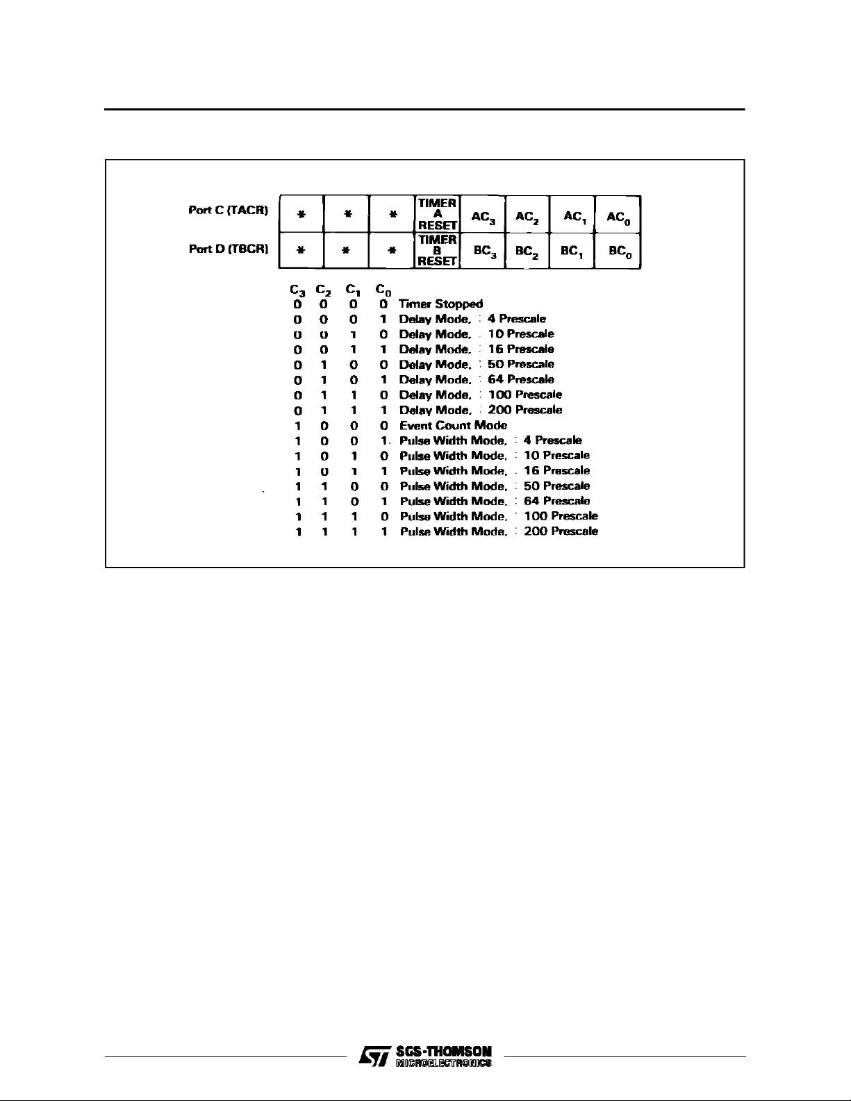
The four timers are programmed via three Timer
ControlRegisters andfourTimerDataRegisters.Timers A and Bare controlledby thecontrol registers
TACRand TBCR,respectively (see figure 12), and
by the data registers TADR and TBDR (figure 13).
TimersCand Darecontrolled bythecontrolregister
TCDCR (see figure 14) and two data registers
TCDR and TDDR. Bits in the control registers allow
the selection of operational mode, prescale, and
controlwhite the data registers are usedto read the
timeror write into the time constant register. Timer
A and B input pins TAI and TBI, are used for the eventand pulse width modes for timers A andB.
Withthe timer stopped, no counting can occur.The
timercontents will remainunaltered while the timer
isstopped(unlessreloaded bywriting the TimerDataRegister), but any residualcount in the prescaler
willbe lost.
9/33
MK68901
Figure 12 : Timer A and B Control Registers.
Unused bits : read as zeros.
*
In the delay mode, the prescaler is always active.
A countpulse will be applied to the main timer unit
each time the prescribed number of timer clock cycles has elapsed. Thus, if the prescaler is programmed to divide by ten, a count pulse will be applied
to the main counter every ten cycles of the timer
clock.
Eachtimeacount pulseisapplied tothemaincounter, it will decrement its contents. The main counter
is initiallyloadedby writingto theTimer Data Register. Each count pulsewillcause the current countto
decrement. When the timerhasdecremented down
to ”01” , the next countpulsewill not cause it to decrement to ”00”. Instead, the next count pulse will
cause the timerto bereloaded from the Timer Data
Register.Additionally, a ”Timeout” pulse willbeproduced. This Time Out pulse is coupled to the timer
interrupt channel, and, if thatchannel is enabled,an
interrupt willbe produced. TheTime Outpulseis also coupled to the timeroutput pin and willcausethe
pin to change states.The output will remain in this
newstateuntilthenextTimeOutpulseoccurs. Thus
the output will complete one full cycle for each two
Time Out pulses.
If, for example, the prescaler were programmed to
divideby ten,andthe TimerData Register wereloa-
V000359
ded with 100(decimal),the main counter would decrement onceforeverytencyclesofthe timerclock.
ATimeOutpulsewilloccur(henceaninterrupt ifthat
channel is enabled) every 1000 cycles of the timer
clock,and thetimer outputwill complete one fullcycleevery 2000 cyclesof thetimer clock.
The maincounter is an 8-bit binary down counter. It
maybe readat any time by reading theTimer Data
Register. The information read is the information
lastclockedintothetimerreadregister when the DS
pinhadlastgonehigh prior to thecurrentreadcycle.
When written,dataisloaded intotheTimerDataRegister,and the main counter, if the timeris stopped.
If the Timer Data Register is written while the timer
is running, thenewwordis notloaded intothe timer
until it counts through H”01”. However, if the timer
iswritten whileitis counting throughH”01”,an indeterminatevalue willbewrittenintothetimer constant
register. This maybecircumvented byensuringthat
the data register is not written when the count is
H”01”.
If the main counter is loaded with ”01”, a Time Out
Pulse will occur every time the prescaler presents
a count pulse to the main counter. If loaded with
”00”, a Time Out pulse will occur every 256 count
pulses.
10/33
 Loading...