

SGS Thomson Microelectronics MK68564 Datasheet
.COMPATIBLEWITH MK68000 CPU
.COMPATIBLEWITH MK68000 SERIESDMA’s
.TWO INDEPENDENT FULL-DUPLEX CHAN-
NELS
.TWO INDEPENDENT BAUD-RATE GENER-
ATORS
Crystaloscillator input
-
Single-phase TTL clockinput
-
.DIRECTLYADDRESSABLE REGISTERS
(all control registers are read/write)
.DATA RATE IN SYNCHRONOUS OR ASYN-
CHRONOUSMODES
0-1.25M bits/second with 5.0MHz system
-
clockrate
.SELF-TEST CAPABILITY
.RECEIVE DATA REGISTERS ARE QUADRU-
PLY BUFFERED ; TRANSMIT REGISTERS
ARE DOUBLY BUFFERED
.DAISY-CHAIN PRIORITY INTERRUPT LOGIC
PROVIDESAUTOMATICINTERRUPTVECTORINGWITHOUT EXTERNAL LOGIC
.MODEM STATUSCAN BE MONITORED
Separate modem controls for each channel
-
.ASYNCHRONOUS FEATURES
5, 6, 7, or 8 bits/character
-
1, 11/2,or 2 stop bits
-
Even, odd, or no parity
-
x1, x16,x32, and x64 clock modes
-
Break generation and detection
-
Parity, overrun, and framingerror detection
-
.BYTE SYNCHRONOUS FEATURES
Internal or external character synchronization
-
Oneor twosynccharacters in separate regis-
-
ters
Automatic sync character insertion
-
CDC-16or CRC-CCITT block check genera-
-
tion and checking
.BIT SYNCHRONOUSFEATURES
Abortsequence generation and detection
-
Automatic zero insertion and deletion
-
Automatic flag insertion between messages
-
Address fieldrecognition
-
I-fieldresidue handling
-
Validreceivemessages protected from over-
-
run
CRC-16or CRC-CCITT block check genera-
-
tion and checking
MK68 56 4
SERIAL INPUTOUTPUT
1
PDIP48
(Plastic Package)
PLCC52
(ChipCarrier)
DESC RIPTION
The MK68564 SIO (Serial Input Output) is a dualchannel, multi-function peripheral circuit, designed
to satisfy a wide variety of serialdata communications requirements in microcomputer systems. Its
basicfunctionisa serial-to-parallel, parallel-to-serial
converter/controller ; however within that role, it is
systemssoftware configurable sothat its ”personality” may be optimized for any given serial data
communications application.
The MK68564 iscapable ofhandling asynchronous
protocols, synchronous byte-oriented protocols
(suchasIBM Bisync), and synchronous bit-oriented
protocols (such asHDLCand IBM SDLC).This versatile device can also be used to support virtually
any serial protocol for applications other than data
communications (cassette or floppy disk interface,
for example).
The MK68564cangenerateand check CRC codes
inany synchronous mode andmay beprogrammed
tocheckdata integrityin variousmodes. Thedevice
also hasfacilities for modem controlsin eachchannel. In applications where these controls are not
needed,the modemcontrolsmaybe used forgeneral-purpose I/O.
January1989
1/46
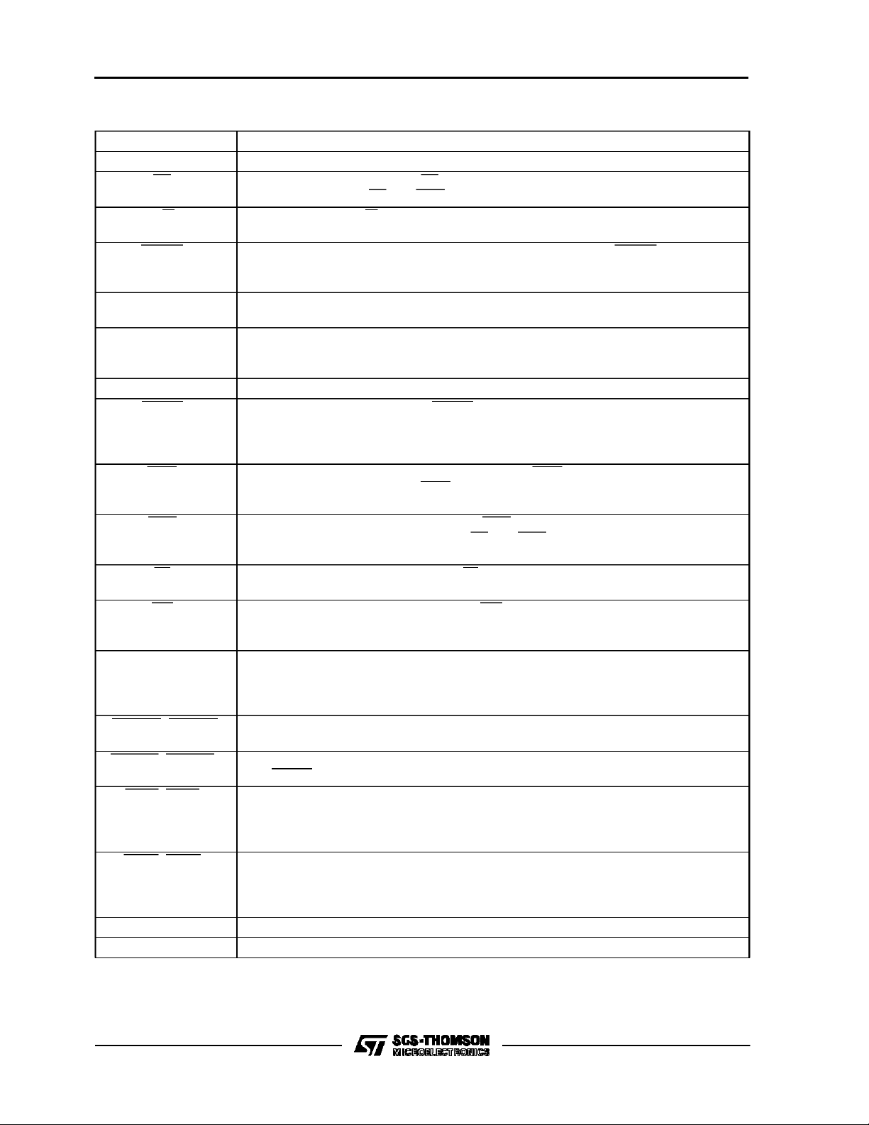
MK 68564
SIO PIN DESCRIPTION
GND : Ground
V
: + 5 Volts (± 5%)
CC
CS : Chip Select (input, active low). CS is used to select the MK68564 SIO for accesses to
the internal registers. CS and IACK must not be asserted at the same time.
R/W : Read/write (input). R/W is the signal from the bus master, indicating wether the current
bus cycle is a Read (high) or Write (low) cycle.
DTACK : Data Transfer Acknowledge (output, active low, three stateable). DTACK is used to
signal the bus master that data is ready or that data has been accepted by the
MK68564 SIO.
A1-A5 : Address Bus (inputs). The address bus is used to select one of the internal registers
during a read or write cycle.
D0-D7 Data Bus (bidirectional, threee-stateable). The data bus is used to transfer data to or
from the internal registers during a read or write cycle. It is also used to pass a vector
during an interrupt acknowledge cycle.
CLK : Clock (input). This input is used to provide the internal timing for the MK68564 SIO.
RESET : Device Reset (input, active low). RESET disables both receivers and transmitters, forces
TxDA and TxDB to a marking condition, forces the modem controls high and disables
all interrupts. With the exception of the status registers, data registers, and the vector
register, all internal registers are cleared. The vector register is reset to ”0FH”.
INTR : Interrupt Request (output, active low, open drain). INTR is asserted when the MK68564
SIO is requesting an interrupt. INTR is negated during an interrupt acknowledge cycle
or by clearing the pending interrupt(s) through software.
IACK : Interrupt acknowledge (input, active low). IACK is used to signal the MK68564 SIO that
the CPU is acknowledging an interrupt. CS and IACK must not be asserted at the same
time.
IEI : Interrupt Enable In (input, active low). IEI is used to signal the MK68564 SIO that no
higher priority device is requesting interrupt service.
IEO : Interrupt Enable Out (output, active low). IEO is used to signal lower priority peripherals
that neither the MK68564 SIO nor another higher priority peripheral is requesting
interrupt service.
XTAL1, XTAL2 : Baud Rate Generator inputs. A crystal may be connected between XTAL1 and XTAL2,
or XTAL1 may be driven with a TTL level clock. When using a crystal, external
capacitors must be connectd. When driving XTAL1 with a TTL level clock, XTAL2 must
be allowed to float.
RxRDYA, RxRDYB: Receiver Ready (outputs, active low). Programmable DMA output for the receiver. The
RxRDY pins pulse low when a character is available in the receive buffer.
TxRDYA, TxRDYB : Transmitter Ready (outputs, active low). Programmable DMA output for the transmitter.
The TxRDY pins pulse low when the transmit buffer is empty.
CTSA, CTSB : Clear to Send (inputs, active low). If Tx Auto Enables is selected, these inputs enable
the transmitter of their respective channels. If Tx Auto Enables is not selected, these
inputs may be used as general purpose input pins. The inputs are Scmit-trigger
buffered to allow slow rise-time input signals.
DCDA, DCDB : Data Carrier Detect (inputs, active low). If Rx Auto Enables is selected, these inputs
enable the receiver of their respective channels. If Rx Auto Enables is not selected,
these inputs may be used as general purpose input pins. The inputs are Schmit-trigger
buffered to allow slow rise-time input signals.
RxDA, RxDB : Receive Data (inputs, active high). Serial data input to the receiver.
TxDA, TxDB : Transmit Data (outputs, active high). Serial data output of the transmitter.
2/46
MK68564
SIO PIN DESCRIPTION (continued)
RxCA, RxCB : Receiver Clocks (input/output). Programmable pin, receive clock input, or baud rate
generator output. The inputs are Schmit-trigger buffered to allow slow rise-time input
signals.
TxCA, TxCB : Transmitter Clocks (input/output). Programmable pin, transmit clock input, or baud rate
generator output. The inputs are Schmit-trigger buffered to allow slow rise-time input
signals.
RTSA, RTSB : Request to Send (outputs, active low). These outputs follow the inverted state
programmed into the RTS bit. When the RTS bit is reset in the asynchronous mode, the
output will not change until the character in the transmitter is completely shifted out.
These pins may be used as general purpose outputs.
DTRA, DTRB : Data Terminal Ready (outputs, Active low). These outputs follow the inverted state
programmed into the DTR bit. These pins may also be used as general purpose
outputs.
SYNCA, SYNCB : Synchronization (input/output, active low). The SYNC pin is an output when Monosync,
Bisync, or SDLC mode is programmed. It is asserted when a sync/flag character is
detected by the receiver. The SYNCpin is a general purpose input in the Asynchronous
mode and an input to the receiver in the External Sync Mode.
Figure 1a: DualIn Line Pin Configuration. Figure 1b : Chip Carrier Pin Configuration.
3/46

MK 68564
SIO SYSTEM INTERFACE
INTRODUCTION
The MK68564 SIO is designed for simple and effi-
cientinterface to a MK68000 CPU system.All data
transfers between the SIOand the CPU are asynchronous tothe system clock. TheSIO system
timing is derived from thechip select input (CS)duringnormalread and write sequences, andfrom the
interrupt acknowledge input (IACK) during an exception processing sequence. CS is a function of
address decode and (normally) lower data strobe
(LDS). IACKisafunction oftheinterruptlevelon address lines A1, A2, and A3, an interrupt acknowledgefunction code(FC0-FC2), and LDS.
Note : CS and IACK can never be asserted at the
sametime.
Note: Unusedinputs should bepulled up or down,
but neverleft floating.
READSEQUENCE
TheSIOwill begin areadcycleif,on thefalling edge
of CS,the read-write (R/W) pin ishigh. The SIO will
respond by decoding the address bus (A1-A5) for
the register selected, byplacingthecontentsof that
register onthedatabuspins(D0-D7),andbydriving
the data transfer acknowledge (DTACK) pin low. If
theregisterselected is not implemented onthe SIO,
the data bus pins will be driven high, and then
DTACK will beasserted. When the CPUhas acquired the data, the CS signal is driven high,at which
time the SIOwill drive DTACK high and thenthreestateDTACK and D0-D7.
WRITESEQUENCE
TheSIOwillbegin awritecycleif, onthefalling edge
of CS, the R/W pin is low. The SIO will respondby
latchingthe data bus,by decoding the address bus
forthe register selected, by loading theregisterwith
the contents of thedata bus,and bydriving DTACK
low. When the CPU hasfinished the cycle, the CS
input is driven high. At this time, the SIO will drive
DTACKhighand will thenthree-state DTACK. If the
register selectedisnotimplemented on theSIO,the
normal write sequence will proceed, but the data
bus contents will not be stored.
INTERRUPT SEQUENCE
The SIO isdesignedto operate asan independent,
interrupting peripheral, or, when interconnected
with other components, an interrupt priority daisy
chaincan beformed.
Independent Operation. Independent operation
requires that the interrupt enable in pin (IEI) be
connected to ground. The SIO starts the interrupt
sequence bydrivingthe interrupt request pin(INTR)
low. The CPUresponds to the interrupt bystarting
an interrupt acknowledge cycle, in which the SIO
IACKpin is driven low. Thehighest priority interrupt
request intheSIO,atthetimeIACKgoeslow,places
itsvectoron thedatabuspins.TheSIOreleasesthe
INTRpinanddrivesDTACKlow.WhentheCPUhas
acquired the vector,the IACK signal is driven high.
The SIO responds bydrivingDTACK toa highlevel
and then three-stating DTACK and D0-D7. If more
than one interrupt request is pending at the start of
an interrupt acknowledge sequence, the SIO will
drive the INTR pin low following the completion of
the interrupt acknowledge cycle.This sequencewill
continue until all pending interrupts are cleared. If
the SIO is not requesting an interrupt when IACK
goeslow,the SIOwill notrespond totheIACKsignal
; DTACKand the data buswill remain three-stated.
DaisyChainOperation. Theinterrupt priority chain
is formed by connecting the interrupt enable out pin
(IEO)of a higher priority part toIEI ofthe next lower
priority part. The highest priority part in the chain
shouldhave IEI tied to ground. The Daisy Chaining
capability (figures 2 and 3) requires that all parts in
a chain have a common IACK signal. When the
commonIACK goes low,all partsfreeze and prioritize interrupts in parallel. Then priority is passed
down the chain, via IEI and IEO, until a part which
has a pending interrupt, once IEI goes low, passes
a vector, does not propagate IEO, and generates
DTACK.
The state of the IEI pin does not affect the SIO interrupt control logic.The SIOcan generate an interruptrequest any time itsinterrupts areenabled. The
IEO pin is normally high ; it will only go low during
anIACKcycleifIEIislowandnointerrupt ispending
intheSIO.TheIEO pin willbe forcedhighwhenever
IACKor IEI goes high.
4/46
Figure 2 : Conceptual Circuit of the MK68564 SIODaisy Chaining Logic.
Figure 3 : Daisy Chaining.
MK68564
V000376
Figure 4 : DMAInterface Timing.
V000377
V000378
5/46

MK 68564
DMA INTERFACE
The SIO isdesigned tointerface tothe68000 family
DMA’sas a 68000 compatible device, using the cycle steal mode. The SIO provides four outputs
(TxRDYA, RxRDYA, TxRDYB, RxRDYB) for requesting servicefrom theDMA.The SIOissuesarequestforservicebypulsingthe RDYpinlowfor three
clock(CLK)cycles(seefigure 4). TxRDY(when enabled) will be active when the transmit buffer becomesempty. RxRDY(whenenabled) willbe active
when a character is available in the receive buffer.
If Receive Interrupt On First Character Only is enabledduring aDMAoperation and aspecial receive
condition is detected, the RxRDY pin will not becomeactive.Instead,a special receive conditioninterrupt will be generated by the channel.
RESET
There aretwo ways of resetting theSIO : an indivi-
dual,programmable channel resetand an external
hardware reset.
The individual channel reset isgenerated by writing
”18H”to theCommandRegister forthe channel selected. All outputs associated with the channel are
resethigh,TxC and RxCareinputs, SYNCisan output,and TxDisforcedmarking.All R/W registers for
the channel areresetto ”00H”, exceptthevectorregisterand the data register, whichare not affected.
Readonlystatusregister1isresetto”01H”(AllSent
set). Break/Abort, Interrupt Pending, and Rx CharacterAvailablebitsin readonlystatus register0 are
reset ; Underrun/EOM, Hunt/Sync, and Tx Buffer
Emptyare set ; CTS andDCD bitsare setto the invertedstate oftheir respective inputpins. Any interruptspendingforthechannel arereset (anypending
interrupts inthe other channel willnot be affected).
Anexternalhardware resetoccurswhenthe RESET
pin is driven low for at least one clock (CLK) cycle.
Both channels are reset as listed above, and the
vector register is reset to ”0FH”.
ARCHITECTURE
The MK68564 SIO contains two independent, full-
duplexchannels. Eachchannel containsatransmitter, receiver, modemcontrol logic, interrupt control
logic, a baud rate generator, ten Read/Write registers,and two read only statusregisters. Eachchannelcan communicatewiththe busmasterusingpolling, interrupts, DMA, or any combination of these
threetechniques. Eachchannel also has theability
toconnect thetransmitteroutputintothereceiverwithout disturbing any external hardware.
Register Set. The register set is the heartof each
channel. A channel is configured for different
communication protocols and interface options by
programming the registers. Table 1 lists all the registersavailablein the SIOand their addresses.
Data Register. The Data Register is composed of
two separate registers : a write only register, which
is the Transmit Buffer, and a read only register,
which is the Receive Buffer. The Receive Buffer is
also the top register of a threeregister stack called
the receive dataFIFO.
Vector Register. The Vector Register is different
from the other 24 registers, because it may be accessedthrough eitherChannel A or Channel B duringa R/W cycle.During an Interrupt Acknowledge
cycle, the contentsof the Vector Register arepassedtotheCPUto beusedasapointertoaninterrupt
serviceroutine. If the StatusAffectsVectorbitisLow
in the Interrupt Control Register, any data written to
the Vector Register will bereturned unmodified duringa Read Cycleor anIACK cycle. Ifthe Status Affects Vector bit is High, the lower three bits of the
vectorreturnedduring aReadorIACKcyclearemodified to reflect the highest priority interrupt pending
in the SIO at thattime. Theupper fivebits writtento
theVector Register areunaffected. Afterahardware
reset only, this register contains a ”0FH” value,
whichistheMK68000’s uninitialized interrupt vector
assignment.
6/46
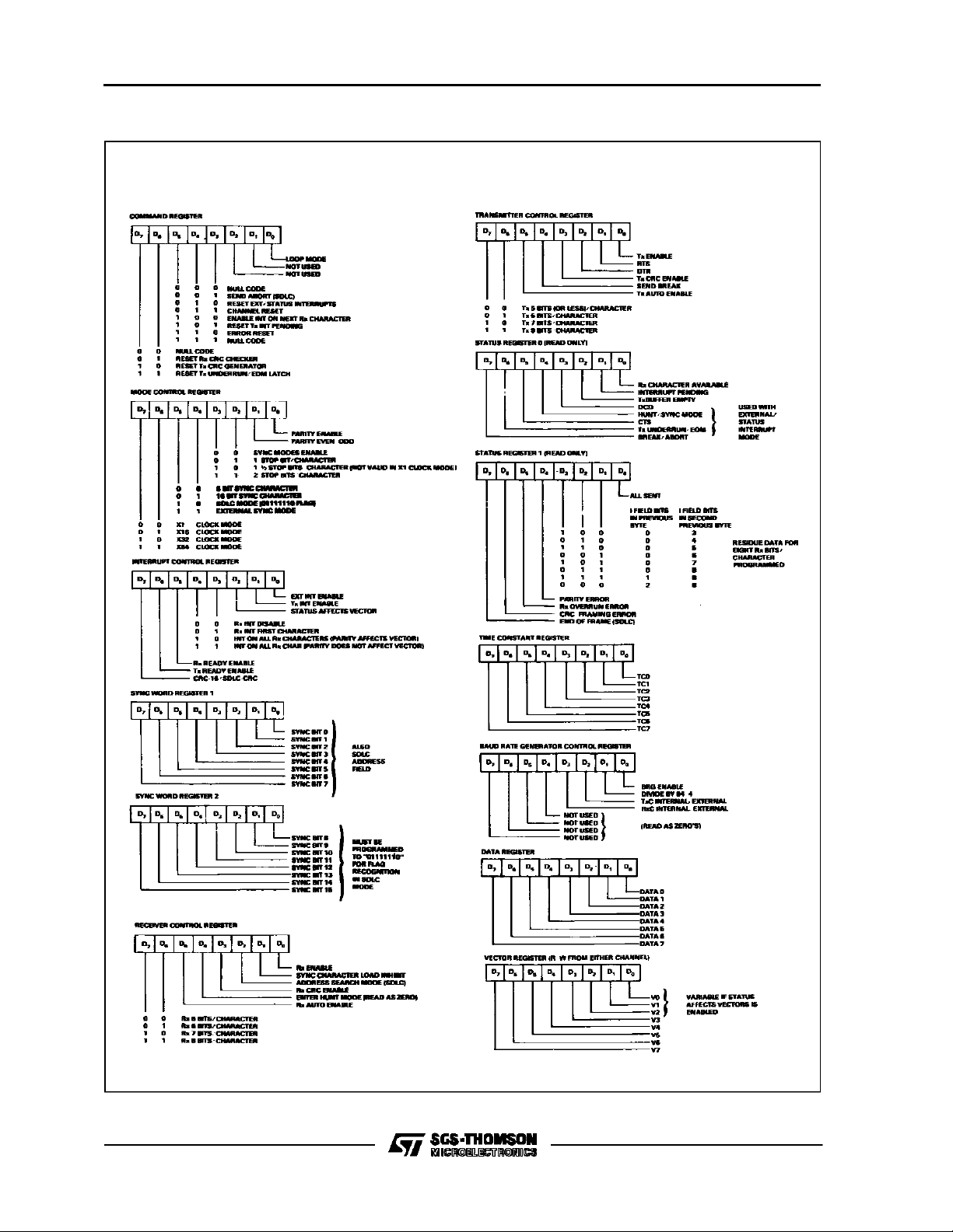
Figure 5 : Register Bit Functions.
MK68564
7/46

MK 68564
SIO INTE RNA L REG IS TERS
The MK68564 SIOhas 25internal registers.Eachchannelhas ten R/W registers andtworeadonly registers
associatedwithit. The vectorregister maybe accessed through eitherchannel.
Table 1 : Register Map.
Address Access
54321
0
0
0
0
0
0
0
0
1
0
0
0
1
0
0
0
0
1
0
0
0
1
0
0
1
1
0
0
1
1
0
0
0
0
1
0
0
0
1
0
1
0
1
0
1
0
1
0
1
1
0
1
0
1
0
1
0
0
1
0
1
0
1
0
1
0
1
0
1
0
1
0
1
1
1
1
1
1
1
1
1
1
1
1
1
1
1
1
1
Notes : 1. Not Used,Read as ”FFH”.
2. Only One Vector Register, Accessible throughEither Channel.
0
0
1
1
1
1
1
0
0
0
0
1
0
1
0
0
1
0
1
1
1
1
1
0
0
0
0
1
0
1
0
0
1
0
1
1
1
1
1
Abbreviati o n Chan nel Regi ster Name
0
1
0
1
0
1
0
1
0
1
0
1
0
1
0
1
0
1
0
1
0
1
0
1
0
1
0
1
0
1
0
1
CMDREG
MODECTL
INTCTL
SYNC 1
SYNC 2
RCVCTL
XMTCTL
STAT 0
STAT 1
DATARG
TCREG
BRGCTL
VECTRG
CMDREG
MODECTL
INTCTL
SYNC 1
SYNC 2
RCVCTL
XMTCTL
STAT 0
STAT 1
DATARG
TCREG
BRGCTL
VECTRG
A
A
A
A
A
A
A
A
A
A
A
A
A/B
A
A
A
B
B
B
B
B
B
B
B
B
B
B
B
A/B
B
B
B
Command Register X
Mode Control Register X
Interrupt Control Register X
Sync Word Register 1 X
Sync Word Register 2 X
Receiver Control Register X
Transmitter Control Register X
Status Register 0 X
Status Register 1 X
Data Register X
Time Constant Register X
Baud Rate Generator Control Reg X
Interrupt Vector Register (note 2) X
(note 1) X
(note 1) X
(note 1) X
Read/
write
Read
Only
8/46
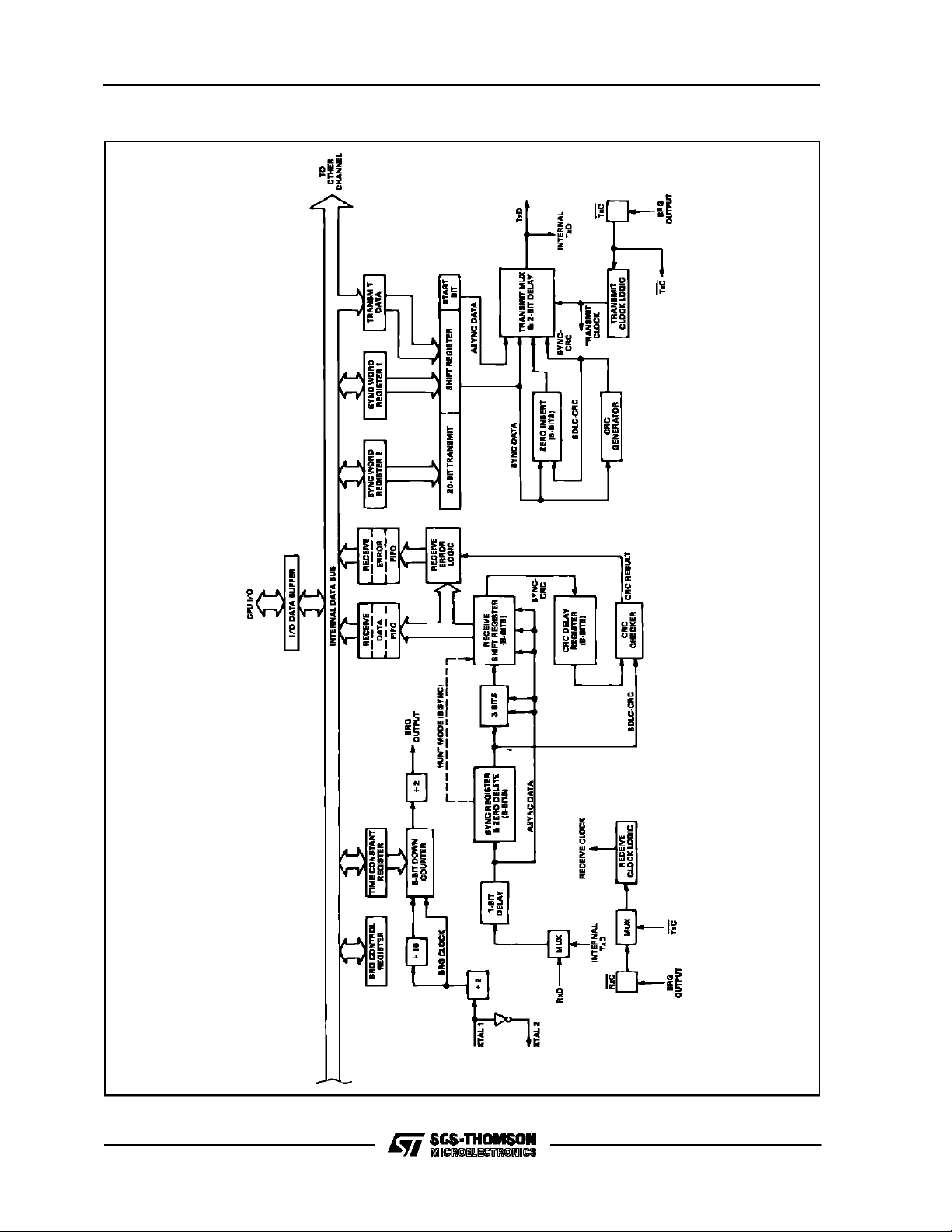
Figure 6 : Transmit and Receive Data Paths.
MK68564
V000379
9/46

MK 68564
DATA PATH
The transmit and receivedata pathsfor each chan-
nel are shown in figure 6. The receiver has three
8-bit buffer registers in a FIFOarrangement (to provide a 3-bytedelay) in addition to the 8-bit receive
shift register. This arrangement creates additional
timefor theCPUtoserviceaninterrupt at thebeginning of ablock of high-speed data. The receiver error FIFO stores parity and framing errors and other
types of status information for each of the three
bytesin thereceive dataFIFO.ThereceiveerrorFIFO is loaded at the same time as the receive data
FIFO. The contents of the receive error are read
throughthe upper four bits in Status Register 1.
Incoming data is routed through one of several
paths,depending onthemodeandcharacterlength.
In the Asynchronous modes, serial data is entered
into the3-bitbuffer, if it hasa character lengthof seven oreight bits,or the data is entered into the 8-bit
receive shift register, if it has a length of fiveor six
bits.
In theSynchronous mode, thedata pathis determinedby thephase ofthe receive process currently in
operation. A Synchronous Receive operation begins with the receiver in the Hunt phase, during
which timethe receiver searches the incomingdata
stream for a bit pattern that matches the preprogrammed sync characters (or flags in the SDLC
mode). If the device is programmed for Monosync
Hunt, amatch is made witha single sync character
stored in Sync Word Register 2. In Bisync Hunt, a
match ismade with the dual sync characters stored
in SyncWord Registers1 and 2. In eithercase, the
incoming data passes through the receive sync register and is compared against the programmed
synccharacters in SyncWord Registers1 and 2.
In the Monosync mode, a matchbetween the sync
character programmed into Sync Word Register 2
andthe character assembled inthereceivesync registerestablishes synchronization.
In the Bysyncmode, incoming data is shiftedto the
receive shift register,while thenext eightbits of the
message are assembled in the receive sync register.The matchbetweentheassembledcharacter in
the syncregister and the programmed character in
Sync Word Register 2, and between the character
in the shift register and the programmed character
in Sync Word Register 1 establishes synchronization.Once synchronization is established,incoming
data bypassesthe receive syncregister anddirectly
entersthe 3-bit buffer.
In the SDLC mode, all incoming data passes
throughthereceivesyncregister,whichcontinuously monitors the receive data stream and performs
zero deletion when indicated. Upon receiving five
contiguous ones, the sixth bit is inspected. If the
sixth bitis a 0, it is deleted from the data stream. If
the sixth bitis a1, the seventhbit isinspected. If the
seventh bit is a 0, a Flag sequence has beenreceived ;ifthe seventh bitisa 1,an Abortsequence has
been received.
The reformatted datafrom thereceive sync register
enters the 3-bit buffer and is transferred to the receiveshift register. Note that theSDLCreceive operationalso begins in the HuntPhase, during which
timetheSIO triesto matchtheassembled character
in the receive sync register with the flag pattern in
SyncWord Register 2. Oncethe firstflag character
is recognized, all subsequent data isroutedthrough
the path described above, regardless of character
length.
Although the same CRC checker is used for both
SDLC and synchronous data, the path taken for
eachmode is different. InBisyncprotocol, the byteoriented operation requires that the CPU decide
whether or not to include the data character in the
CRC calculation. To allow the CPU ample time to
make this decision, the SIO provides an 8-bit delay
before the data enters the CRC checker. In the
SDLCmode,nodelayis provided, since CRCiscalculated onall data betweentheopening and closing
flags.
The transmitter has an 8-bittransmit data register,
which is loaded from the internalbus, and a 20-bit
transmit shift register, which can be loaded from
Sync Word Register1, Sync Word Register 2, and
the transmit data register. Sync Word Registers 1
and 2 contain sync characters in the Monosync, Bisync,orExternal Sync modes, oraddress field (one
character long) and flag, respectively, in the SDLC
mode. During Synchronous modes, information
contained in Sync WordRegisters 1 and2is loaded
intothe transmit shift registerat the beginning of the
message and, as a time filler, in the middle of the
message if a Transmit Underrun condition occurs.
InSDLCmode,theflags areloaded intothetransmit
shift register at the beginning and endof the message.
Asynchronous data in the transmit shift register is
formattedwith startandstopbits,and itisshiftedout
tothe transmit multiplexer attheselected clockrate.
Synchronous (Monosync, Bisync, or External Sync)
data isshiftedoutto the transmit multiplexer and also the CRC generator at the x1 clock rate.
SDLC/HDLC data isshiftedout throughthe zeroinsertionlogic,whichis disabled while flags are being
sent.Forallotherfields (address, control, andframe
check),a 0isinsertedfollowingfivecontiguousones
10/46

MK68564
in the data stream. Notethat theCRC generator result (frame check) for SDLC data is also routed
throughthe zero insertion logic.
I/O CAPABILITIES
The SIOoffers the choiceof Polling, Interrupt (vec-
toredor non-vectored), and DMATransfermodesto
transfer data, status, and control information toand
from the CPUor other bus master.
Polling.The Polledmode avoids interrupts. Status
Registers 0 and1 are updated at appropriate times
for each function being performed (for example,
CRC Errorstatus valid at the end of themessage).
All theinterrupt modesof the SIO must be
disabled to operate the device in a polled environment.
While initsPollingsequence, theCPUexamines the
statuscontained inStatus Register 0foreachchannel. Thestate of the statusbits in StatusRegister0
servesas anacknowledgetothePollinquiry. Status
bitsD0andD2 indicatethata receive ortransmitdata transfer is needed. The rest of the status bitsin
StatusRegister0 indicate special statusconditions.
The receiver error condition bits in Status Register
1 donothave tobereaduntiltheRxCharacter Availablestatus bit in StatusRegister 0 isset to a one.
Interrupts. The SIO offers an elaborate interrupt
scheme to provide fast interrupt response in realtime applications. The interrupt vector points to an
interrupt serviceroutine in the memory. To service
operations inboth channels and to eliminate thenecessityof writing a statusanalysis routine (asrequiredfora polling scheme), the SIOcanmodifytheinterrupt vectorsoitpointstooneofeight interrupt serviceroutines. Thisis done underprogram control by
setting theStatus AffectsVector bit in the Interrupt
Control Register ofchannel Aorchannel B,toaone.
When thisbit isset, the interrupt vector is modified
according to the assigned priority of the various interrupting conditions.
Note: If theStatus Affects Vector bit is set in either
channel, the vector is modified for both channels.
Thisis the onlycontrolbit thatoperates inthis mannerin the SIO.
Transmit interrupts, Receive interrupts, and External/Status interrupts are the sources of interrupts.
Each interrupt source is enabled under program
controlwith Channel Ahaving a higher priority than
Channel B, and withReceiver,Transmitter, andExternal/Statusinterrupts prioritizedin thatorder within
each channel. When the Transmit interrupt is enabled, theCPU is interrupted by the transmit buffer
becoming empty. This implies that the transmitter
must have had a data character written into it so t
canbecome empty.Whenenabled, thereceiver can
interrupt the CPU in one of threeways :
Interrupt OnFirst CharacterOnly
Interrupt OnAll Receive Characters
Interrupt OnA Special Receive Condition.
Interrupt On First Character Only.This mode is
normally used to start a software Polling loop or a
DMA transfer routine using the RxRDY pin. In this
mode, the SIO generates an interrupt on the first
character received after this mode is selected and,
thereafter, only generates an interrupt if a Special
Receive Condition occurs. The Special Receive
Conditions that can causean interrupt in this mode
are: Rx OverrunError,Framing Error (in Asynchronousmodes), and EndOf Frame (in SDLCmode).
Thismode isreinitialized bytheEnable Interrupt On
Next Rx Character command.If a Special Receive
Condition interrupt occursinthis interrupt mode,the
data withthe special conditionis held inthe receive
data FIFOuntilan Error Reset Command isissued.
InterruptOnAll ReceiveCharacters. Inthismode,
an interrupt is generated whenever thereceivedata
FIFO contains a character or a Special Receive
Condition occurs. The Special Receive Conditions
thatcan cause an interrupt in thismode are : Rx Overrun Error, Framing Error (in Asynchronous
modes), End ofFrame (in SDLC mode),and Parity
Error (if selected).
Interrupt On A Special Receive Condition. The
Special Receive Condition interrupt is not,as such,
a separate interrupt mode. Before a Special ReceiveCondition can cause aninterrupt, either theInterrupt On First Character Only or Interrupt On All
Receive Characters mode must be selected. The
Special Receive Condition interrupt will modify the
receive interrupt vectorifStatusAffectsVector isenabled.The Special Receive Condition status is displayed in the upper four bits of Status Register 1.
Two of the conditions causing a special receive interrupt arelatched whentheyoccur;they are:Parity
Error and Rx Overrun Error. These statusbits may
onlybe reset byan Error Reset command. Wheneither of these conditions occur,a read of StatusRegister 1 will reflect any errorsin the currentword in
the receive buffer plus any parity or overrun errors
sincethe last Error Reset command wasissued.
External/Status Interrupts. The main function of
the External/Status interrupt is to monitor thesignal
transitions of theCTS, DCD,and SYNCpins ; however, anExternal/Status interrupt is alsocaused by
a TransmitUnderrun condition orby thedetection of
a Break (Asynchronous mode) or Abort (SDLC
mode)sequence in thereceived datastream.When
any one of the above conditions occur, the exter-
11/46
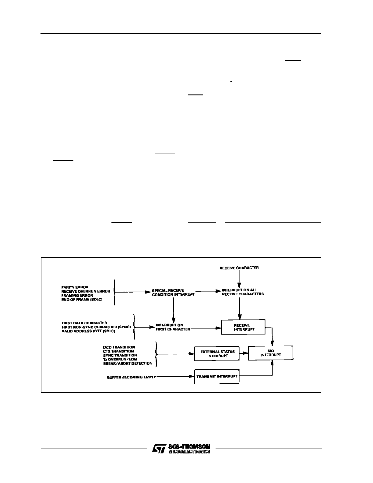
MK 68564
nal/status logiclatches thecurrent stateof allfiveinput conditions, andgenerates an interrupt. Toreinitialize the external/status logic to detect another
transition, a Reset External/Status Interrupts
command must be issued. The Break/Abort conditionallows theSIOtogenerate aninterrupt whenthe
Break/Abort sequence is detectedand terminated.
This featurefacilitates the proper termination of the
current message, correct initialization of the next
message, and the accurate timing of the Break/Abortcondition inexternal logic.
DMA Transfer
TheSIOprovides twooutput signals perchannelfor
connection to a DMA controller ; they are TxRDY
and RxRDY. The outputs are enabled under software control by writing tothe Interrupt Control Register. Both outputs willpulse Low for three system
clock cycleswhen their input conditions are active.
TxRDYwill be active whenthe Transmit Buffer
becomesempty.RxRDYwillbe activewhen acharacter isavailable in theReceive Buffer. If a Special
Receive Condition occurs when Interrupt On First
Character Only mode is selected, a receiver interrupt will be generated and RxRDY willnot become
active. This will automatically inform the CPU of a
discrepancy in the data transfer.
SELFTEST
Whenthe LoopModebit issetin theCommandRe-
gister,thereceiver shiftclockinputpin(RxC)andthe
receiver data input pin (RxD) are electrically disconnected from theinternal logic. Thetransmitdata
output pin (TxD)is connected to the internal
receiver data logic, and the transmit shift clock pin
(TxC)isconnected totheinternal receivershiftclock
logic.All other features of the SIO are unaffected.
BAUDRATE GENERATORS
Each channelin theSIO contains a programmable
baud rate generator (BRG). Each BRG consists of
an 8-bit timeconstant register, an 8-bit downcounter,a controlregister, anda flip-flop onthe output to
provide a square wave signalout. In addition tothe
flip-flopon the output, thereis alsoa flip-flop on the
inputclock;therefore, themaximum outputfrequency of theBRGisone-forth oftheinputclockfrequency. Thismaximum output frequency occurs when
divide by four mode is selected, and the time
constant register is loaded with theminimum count
of ”01H”. The equation to determine the output frequencyis :
Output
=
Input Frequency
Frequency (divideby selected)X (time constant
value in decimal)
Figure 7 : InterruptStructure.
V000380
12/46
MK68564
Forexample,whenthe timeconstant registerisloaded with ”01H” and divide by four is selected, one
outputclock will occur for every four input clocks.If
the time constant value loaded is ”00H” (256 decimal) instead of ”01H” and divide by 64 is selected,
one output clock will occur for every 16384 input
clocks.Note that theminimum count value is”01H”
(1 decimal), and the maximum count valueis ”00H”
(256 decimal).
The output of the baud rate generator may be programmed to drive the transmitter (BRG output on
TxC),the receiver(BRGoutputon RxC), both (BRG
output on TxC and RxC), or neither(TxC and RxC
areinputs). Aftera reset, thebaud rate generator is
disabled, divide by four is selected, and TxC and
RxC are inputs.
The baudrate generator should be disabled before
the CPUwrites tothe time constantregister. Thisis
necessary because no attempt was made to synchronize the loading of anew timeconstant with the
clockused to drive the BRG.
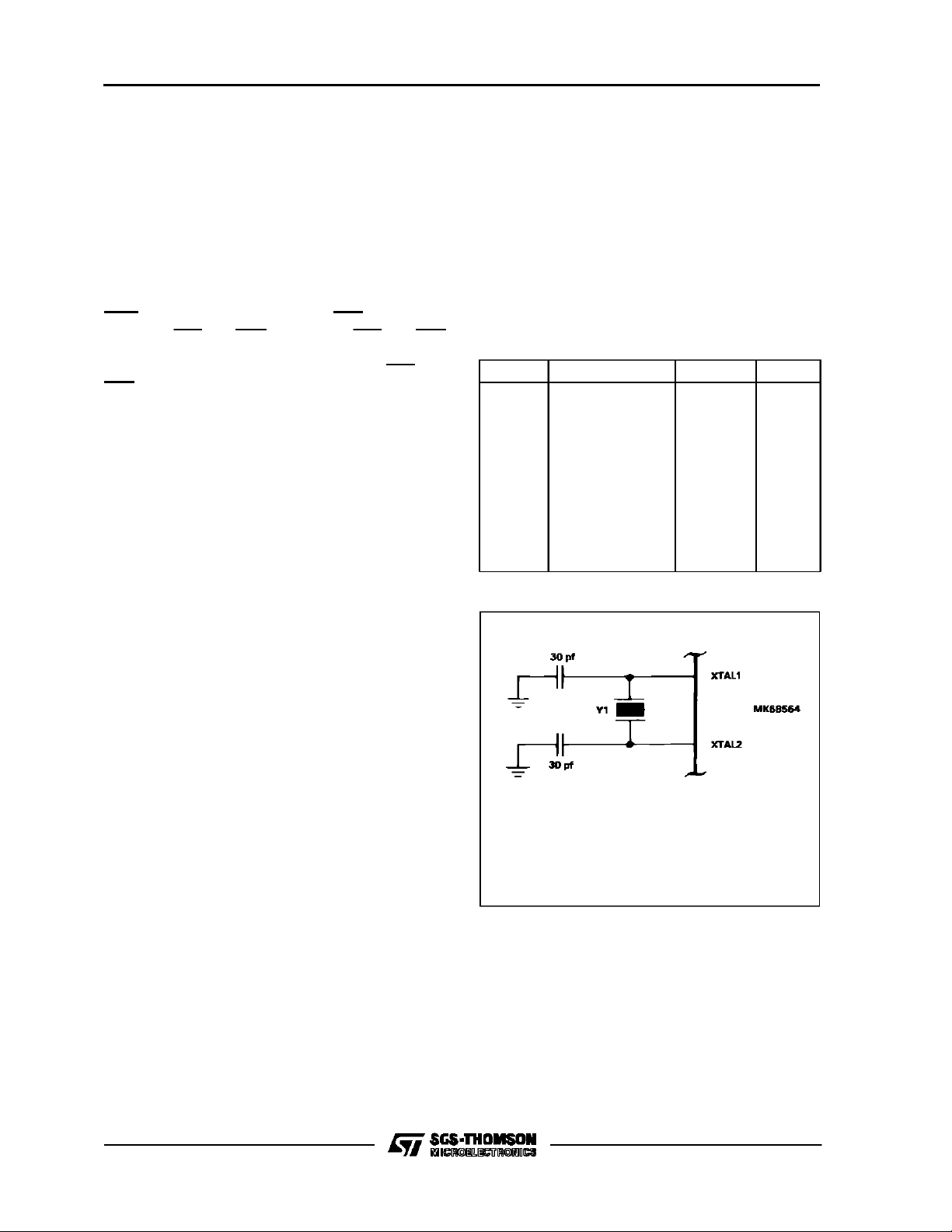
Figure 8indicates the externalcomponents needed
to connect a crystal oscillator to the SIO XTAL inputs.Theallowed crystalparameters arealsolisted.
For a 3.6864MHz input signal to the baud rate generator,thetime constants, listed in table2, areloaded to obtain the desired baud rates (in x1 clock
mode).
To set up the SIOfor Asynchronous operation, the
following registers need to be initialized : Mode
ControlRegister, Interrupt Control Register, Receiver Control Register, and Transmitter Control
Register. The Mode Control Register must be
programmed before the other registers to assure
properoperation ofthe SIO. The following registers
are used to transferdata or tocommunicate status
between the SIOand the CPU or other bus master
when operating in Asynchronous modes :
Command Register, Status Register 0, Status Register 1, DataRegister, and theVector Register.
Table 2 : Time-ConstantValues.
Ra t e Ti m e Constant Divi de By Error
19200
9600
7200
4800
3600
2400
2000
1800
1200
600
300
Figure8 :
48
96
128
192
256
24
29
32
48
96
192
SIO External Oscillator Components.
4
4
4
4
4
64
64
64
64
64
64
69 %
ASYNCHRO N OU S OPERAT ION
INTRODUCTION
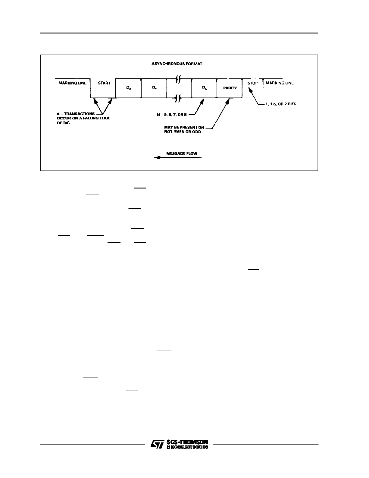
Manytypesof Asynchronous operations are performed by the MK68564 SIO.Figure 9 represents a ty-
pical Asynchronous message format and some of
the options available on the SIO. Thetransmit processinserts start, stop, and parity bitsto a variable
data format and supplies a serialdata streamto the
Transmit Dataoutput(TxD). The receiver takesthe
data from the Receive Data input (RxD) and strips
awayexpectedstart andstop bitsat a programmed
clockrate. Itprovideserror checking foroverrun,parity, and carrier-loss errors,and, ifdesired,provides
interrupts forthese conditions.
CRYSTALPARAMETERS :
Parallel Resonance, FundamentalMode AT Cut
Rs â150Ω(Fr = 2.8- 5.0MHz)
Rs â300Ω(Fr = 2.0- 2.7MHz)
CI = 18pf ; Cm = 0.02pF ; Ch= 5pF ; Lm = 96MHz
Fr (typ)= 2.457MHz
13/46
MK 68564
Figure 9 : Asynchronous MessageFormat.
V000382
The SIOprovides fiveI/O linesthatmay beused for
modemcontrol, forexternalinterrupts, oras general
purpose I/O.The Request To Send(RTS) and Data
Terminal Ready (DTR) pins are outputs that follow
the inverted state of their respective bits in the
Transmitter ControlRegister.The RTS pin canalso
be usedto signal theendof a message inAsynchronous modes, as explained below in the transmitter
section. The Data Carrier Detect (DCD), Clear To
Send (CTS), and SYNC pins are inputs to the SIO
in Asynchronous modes. DCD and CTS can be used as auto enablesto thereceiver and transmitter,
respectively, or if External/Status Interruptsare enabled all three input pins will be monitored for a
change ofstatus.If these inputs change fora period
of time greater than the minimum specified pulse
width,an interrupt will be generated.
In the following discussion,all interrupt modes are
assumed enabled.
ASYNCHRONOUS TRANSMIT
Start of Transmission. TheSIO willstart transmit-
ting data when the Transmit Enable bit is set to a
one,anda characterhasbeenloaded intothe transmit buffer. If the TxAutoEnables bit is set,the SIO
willwait fora Low on the ClearToSend input(CTS)
beforestarting data transmission.The TxAuto Enables feature allows the programmer to send the
first data character of the message to the SIO without waiting for CTS to go Low. In all cases, the
Transmit Enable bitmustbesetbeforetransmission
can begin. Thetransitions on the CTSpin will generate External/Status interrupt requests and also
latch up the external/status logic. The external/status logic should be rearmed by issuing a ResetExternal/Status Interruptscommand.
Transmit Characteristics. The SIO automatically
inserts astartbit, theprogrammed parity bit(odd,even, or no parity),and the programmed number of
stopbitstothe data character tobetransmitted. The
transmitter can transmit from one to eight data bits
per character. All characters are transmitted leastsignificant bit first. When the character length programmed issix orseven bits, the unused bits of the
transmit buffer are automatically ignored. When a
character length of fivebits or less is programmed,
the data loaded into the transmit buffermust be formatted as described in the Transmitter Control RegisterpartoftheRegisterDescriptionsection. Serial
data isshifted out of the TxD pin onthe falling edge
of the Transmit Clock (TxC) at a rate equal to 1,
1/16th, 1/32nd, or 1/64th of TxC.
Data Transfer. The SIO will signal the CPUorother
bus master witha transmitinterrupt request andset
the Tx Buffer Empty bit in StatusRegister 0,every
time the contents of the transmit buffer are loaded
intothe transmit shift register.The interrupt request
will becleared when a newcharacter is loaded into
the transmit buffer, or a ResetTx InterruptPending
command(Command 5) is issued. If Command 5 is
issued, thetransmitbufferwillhaveto be loaded before any additional transmit interrupt requests are
generated. The Tx Buffer Empty bitis reset whena
new character is loaded into the transmit buffer.
The AllSent bit inStatusRegister 1 is used to indicate when all data in the shift register has been
transmitted,and thetransmitbufferisempty.Thisbit
is Low, while the transmitter issending characters,
anditwill goHighonebittime afterthetransmitclock
that clocks out the last stop bit of the character on
the TxD pin. No interruptsare generated by the All
Sentbit transitions. TheRequest ToSend(RTS) bit
14/46
 Loading...