

SGS Thomson Microelectronics MK50H28N, MK50H28Q Datasheet

MK50H28
MULTI LOGICAL LINK
FRAME RELAY CONTROLLER
SECTION1 - FEATURES
Based on ITU Q.933 Annex A and T1.617 Annex D Standards for Frame Relay Service and
Additional Pocedures for Permanent Virtual
Circuits(PVCs).
Optional Transparent Mode (no LMI Protocol
Processing- all frame data received).
Local Management Link Protocol with optional
Bi-directionalmessageprocessing.
Detects and indicates service-affecting errors
in the timingorcontent of events.
Programmable Timers/Counters: nT1/T391,
nT2/T392, nN1/N391, nN2/N392, nN3/N393
and dN1for the LMI/LIV channel.
Provides Error Counters for the LMI channel
and Congestion Statistics for all the active
channels.
LMI/LIV Frames can be transmitted/received
on DLCI0 or 1023.
Supportsreception of up to 4 octetsof address
field with a maximum of 8192 active channels
or DLCIs (Data Link Connection Identifiers)
Priority DLCI scheme for channels requiring
higher rate of service.
BufferManagementincludes:
- InitializationBlock
- AddressLook Up Table
- ContextTable
- SeparateReceiveand Transmit Rings of variable sizefor each activechannel
On chip DMA control with programmableburst
length.
Handles all HDLC frame formatting:
- Zerobit insertion and deletion
- FCS(CRC) generationand detection
- Framedelimiting with flags
Programmable minimum frame spacing on
transmission(1-62 flags between frames).
SelectableFCS (CRC) of 16 or 32bits.
Testing Facilities: Internal Loopback, Silent
Loopback,ClocklessLoopback,and SelfTest.
Systemclock rates up to 25 MHz.
CMOS process; Fully compatible with both 8
and 16 bit systems;All inputs and outputs are
TTL compatible.
Programmablefor full or half duplexoperation.
Pin-for-pin compatible and architecturally the
same as the MK50H25 (X.25/LAPD) and
MK50H27(CCS#7).
SECTION2 - DESCRIPTION
The STMicroelectronics MK50H28 Multi-Logical
Link Communications Controller is a CMOS VLSI
devicewhich provides link level data communications control for Frame Relay Applicationson Permanent Virtual Circuits (PVCs). The MK50H28
will perform frame formating including: frame delimiting with flags, transparency (so-called ”bitstuffing”), plus FCS (CRC) generation and detection. It also supports Local ManagementInterface
(LMI)protocol with the ”Optional Bidirectional Procedures” (Annex D, T1.617 - 1991 and T1.617a-
1994).
One of the outstanding features of the MK50H28
is its buffer management which includes on-chip
dual channel DMA. This feature allows users to
receive and transmit multiple data frames at a
time. (A conventional serial communicationscontrol chip plus a separate DMA chip would handle
data for only a single block at a time.) The
March 2000
DIP48
PLCC52
1/64
MK50H28 will move multiple blocks of receive
and transmit data directly into and out of memory
through the Host’s bus. Moreover, the memory
management capability includes the chaining of
long frames. A possible system configuration for
the MK50H28 is shown in Figure 1.
The MK50H28 may be used with any of several
popular 16 and 8 bit microprocessors, such as
68000, 6800, Z8000, Z80, LSI- 11, 8086, 8088,
8080,etc.
The MK50H28 may be operated in either full or
half duplex mode. In half duplex mode, the RTS
and CTS modem control pins are provided. In full
duplex mode, these pins become user programmable I/O pins. All signal pins on the MK50H28
are TTL compatible. This has the advantage of
makingthe MK50H28independentof the physical
interface. As shown in Figure 1, line drivers and
receivers are used for electrical connectionto the
physicallayer.
DESCRIPTION(Continued)
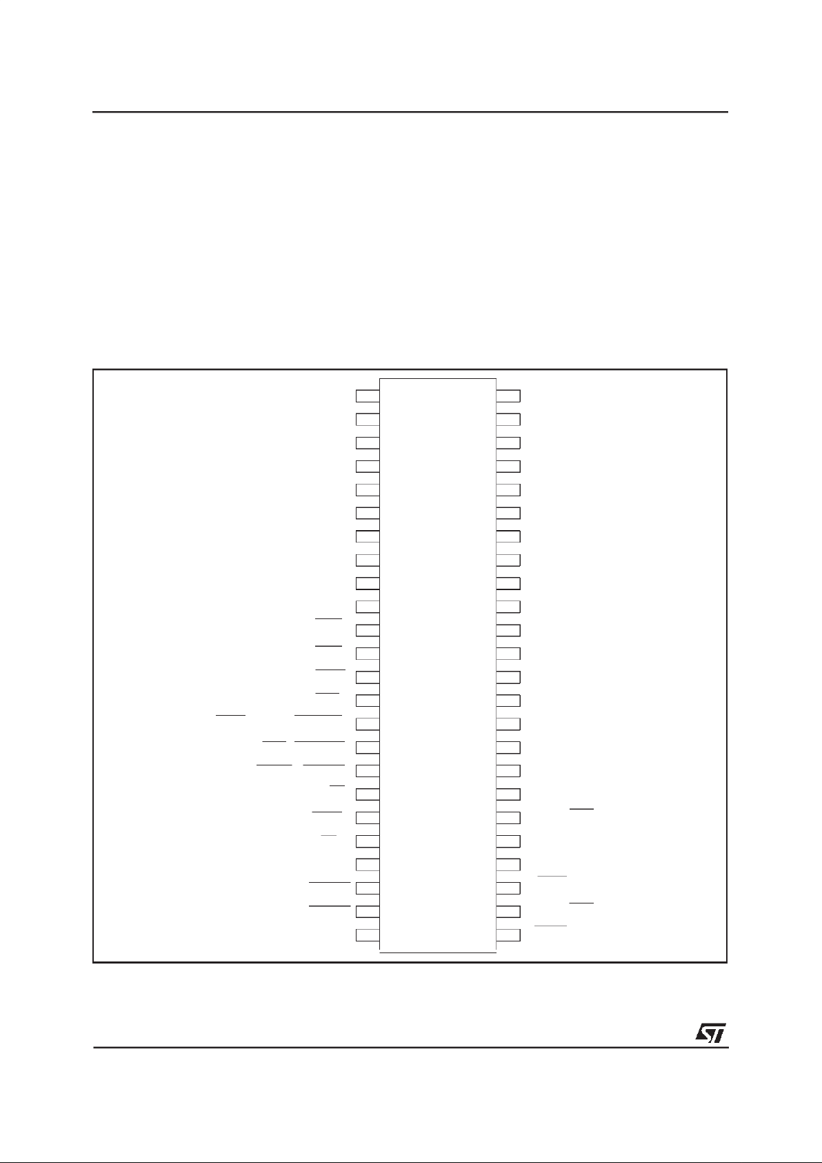
VSS-GND
DAL07
DAL06
DAL05
DAL04
DAL03
DAL02
DAL01
DAL00
READ
INTR
DALI
DALO
DAS
BMO, BYTE, BUSREL
BMI, BUSAKO
HOLD, BUSRQ
ALE, AS
CS
ADR
READY
RESET
VSS-GND
24
HLDA
1
2
3
4
5
6
7
8
9
10
11
12
13
14
48
47
46
45
44
43
42
41
40
39
38
37
36
23
22
21
20
19
18
17
16
15
35
34
33
32
31
30
29
28
27
26
25
TCLK
A18
A19
A20
A21
A22
A23
RD
DSR, CTS
TD
SYSCLK
RCLK
DTR, RTS
VCC (+5V)
DAL08
DAL09
DAL10
DAL11
DAL12
DAL13
DAL14
DAL15
A16
A17
M
K
5
0
H
2
8
DIP48 PIN CONNECTION (Top view)
MK50H28
2/64
GND
DAL07
DAL06
DAL05
DAL04
DAL03
DAL02
DAL01
DAL00
READ
INTR
DALI
DALO
DAS
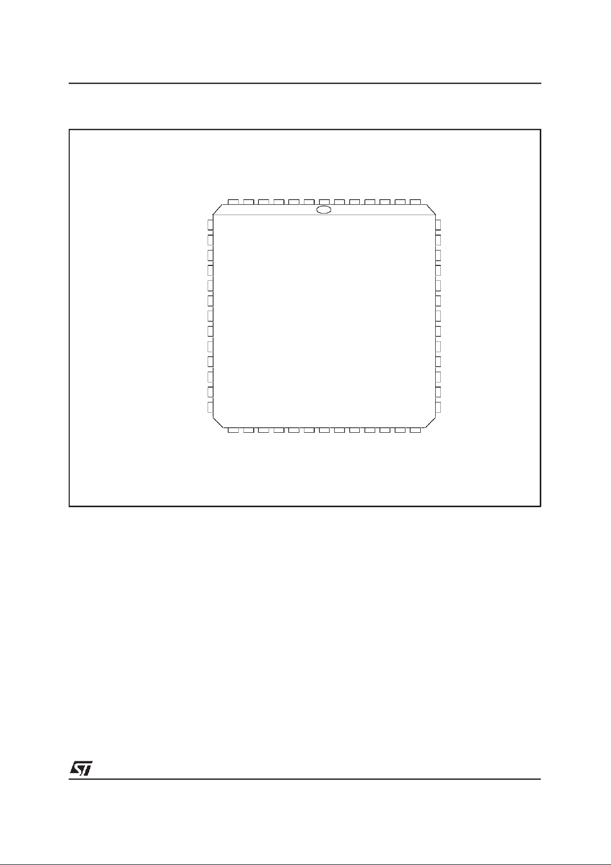
8
7 1 52 47
46
34
33
21
20
BMO/BYTE/BUSREL
No Connect
BM1/BUSAKO
HOLD/BUSRQ
ALE/AS
HLDA
CS
ADR
READY
RESET
GND
TCLK
No Connect
DTR/RTS
RCLK
SYSCLK
TD
DSR/CTS
RD
A23
No Connect
A22
A21
A20
A19
A18
A17
A16
DAL15
DAL13
DAL14
VCC
DAL08
DAL09
DAL10
DAL11
DAL12
No Connect
MK50H28Q
PLCC52 PIN CONNECTION(Top view)
MK50H28
3/64
SIGNAL NAME PIN(S) TYPE DESCRIPTION
DAL<15:00> 2-9
40-47
[2-10
44-51]
IO/3S The time multiplexed Data/Addressbus. During theaddress portion of a
memory transfer, DAL<15:00> contains the lower16 bits of the memory
address.
During the data portion of a memory transfer, DAL<15:00> contains the read
or write data, depending on the typeof transfer.
READ 10
[11]
IO/3S READ indicatesthe type of operation that the bus controller is performing
during abus transaction. READ is driven by the MK50H28 only while it isthe
BUS MASTER. READ isvalid during the entire bus transaction and is
tristated at all other times.
MK50H28 as a BusSlave :
READ = HIGH - Data is placed on the DAL linesby the chip.
READ = LOW - Data is taken off the DAL lines bythe chip.
MK50H28 as a BusMaster :
READ = HIGH - Data is taken off theDAL lines by the chip.
READ = LOW - Data is placed on the DAL lines by the chip.
INTR 11
[12]
O/OD INTERRUPT is an attention interrupt line that indicates thatone or more of
the following CSR0 status flags is set: MISS, MERR, RINT, TINT or PINT.
INTERRUPT is enabled by CSR0<09>, INEA=1.
DALI 12
[13]
O/3S DALIN is an external bus transceiver control line. DALI is drivenby the
MK50H28 only while it is the BUS MASTER. DALIis asserted by the
MK50H28 when it readsfrom the DAL lines during the data portion of a
READ transfer. DALIis not asserted during a WRITE transfer.
DALO 13
[14]
O/3S DALOUT is an external bus transceiver control line. DALO is driven by the
MK50H28 only while it is the BUS MASTER. DALO is asserted by the
MK50H28 when it drivesthe DAL linesduring the address portionof a READ
transfer or for the durationof aWRITE transfer.
DAS 14
[15]
IO/3S DATA STROBE defines the data portion of a bus transaction. By definition,
data is stable and valid at the low tohigh transition of DAS. This signal is
driven by the MK50H28 while it is the BUS MASTER. Duringthe BUS
SLAVE operation, this pin is used as an input. At all other times the signal is
tristated.
BMO
BYTE
BUSREL
15
[16]
IO/3S I/O pins 15 and 16 are programmable through CSR4. If bit06 of CSR4 is set
to a one, pin 15 becomes input BUSREL and is usedby the host to signal
the MK50H28 to terminate a DMA burst after the current bus transfer has
completed. If bit 06 is clear then pin 15 is an outputand behavesas
described belowfor pin16.
BM1
BUSAKO
16
[18]
O/3S Pins15 and 16 are programmable through bit 00 of CSR4 (BCON).
If CSR4<00> BCON = 0,
I/O PIN 15 = BMO (O/3S)
I/O PIN 16 = BM1 (O/3S)
BYTE MASK<1:0> Indicates the byte(s) on the DAL to be read or written
during thisbus transaction. MK50H28 drives these lines only as a Bus
Master. MK50H28 ignores the BM lineswhen it is a Bus Slave.
Byte selectionis done as outlined in the following table.
BM1 BM0 TYPE OF TRANSFER
LOW LOW ENTIRE WORD
LOW HIGH UPPER BYTE
(DAL<15:08>)
HIGH LOW LOWER BYTE
(DAL<07:00>)
HIGH HIGH NONE
TAble 1 - PIN DESCRIPTION
LEGEND:
I Inputonly O Outputonly
IO Input/ Output 3S 3-State
OD OpenDrain (no internalpull-up)
Note: Pin out for 52 pin PLCCis shown in brackets.
MK50H28
4/64
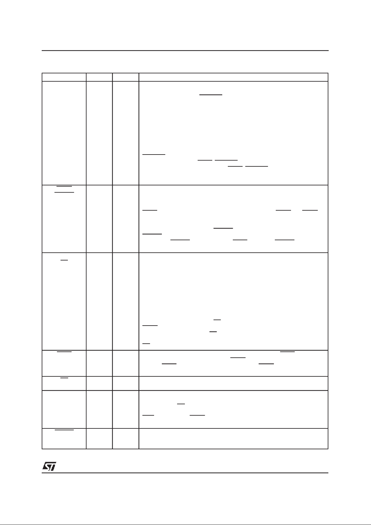
Table 1: PIN DESCRIPTION(continued)
SIGNAL NAME PIN(S) TYPE DESCRIPTION
If CSR4<00> BCON = 1,
I/O PIN 15 = BYTE (O/3S)
I/O PIN 16 = BUSAKO(O)
Byte selectionis done using the BYTE line and DAL<00> latched during the
address portion of thebus transaction. MK50H28 drives BYTE onlyas a Bus
Master and ignores it when a Bus Slave. Byte selection is done as outlined
in thefollowing table.
BYTE DAL<00> TYPE OF TRANSFER
LOW LOW ENTIRE WORD
LOW HIGH ILLEGAL CONDITION
HIGH LOW LOWER BYTE
HIGH HIGH UPPER BYTE
BUSAKOis a bus request daisy chainoutput. If MK50H28 is not requesting
the bus and it receives HLDA, BUSAKOwill be driven low. If MK50H28is
requesting the bus when it receives HLDA, BUSAKO will remain high
Note: All transfers are entireword unless the MK50H28 is configured for 8 bit
operation.
HOLD
BUSRQ
17
[19]
IO/OD Pin 17 is configured through bit 0 of CSR4.
If CSR4<00> BCON = 0,
I/O PIN 17 = HOLD
HOLD requestis assertedby MK50H28 when it requires a DMA cycle, if
HLDA is inactive, regardless of the previousstate of the HOLD pin. HOLD is
held low for the entireensuing bustransaction.
If CSR4<00> BCON = 1,
I/O PIN 17 = BUSRQ
BUSRQis asserted by MK50H28 when it requires a DMA cycle ifthe prior
state ofthe BUSRQ pin was high and HLDA is inactive. BUSRQ is held low
for the entire ensuing bus transaction.
ALE
AS
18
[20]
O/3S Theactive level of ADDRESS STROBE is programmablethrough CSR4.
The address portion of a bustransfer occurs while this signal isat its
asserted level.This signal is driven by MK50H28 whileit is theBUS
MASTER. At all other times, the signalis tristated.
If CSR4<01> ACON = 0,
I/O PIN 18 = ALE
ADDRESS LATCH ENABLE isused to demultiplex the DAL lines anddefine
the address portion of the transfer. As ALE, the signaltransitions from high
to low during the address portion of the transferand remains low during the
data portion.
If CSR4<01> ACON = 1,
I/O PIN 18 = AS
AsAS, the signal pulses low during the address portion of the bus transfer.
The low to hightransition of AS can beused by a slave deviceto strobe the
address into a register.
ASis effectively the inversion of ALE.
HLDA 19
[21]
I HOLD ACKNOWLEDGE is theresponse to HOLD. When HLDA is low in
response to MK50H28’s assertion of HOLD, the MK50H28 is theBus
Master. HLDA should bedeasserted ONLY after HOLD has been released
by the MK50H28.
CS 20
[22]
I CHIP SELECT indicates, when low, that theMK50H28 is the slave device
for the data transfer. CS must bevalid throughout the entire transaction.
ADR 21
[23]
I ADDRESS selects the Register Address Port or the Register Data Port. It
must be valid throughout thedata portion of the transfer and is only used by
the chip when CS is low.
ADR PORT
LOW REGISTER DATA PORT
HIGH REGISTER ADDRESS PORT
READY 22
[24]
IO/OD When the MK50H28 is a Bus Master, READY is an asynchronous
acknowledgement from the busmemory that memory willaccept data in a
WRITE cycle or thatmemory hasput data on the DAL lines in a READ cycle.
MK50H28
5/64
Table 1: PIN DESCRIPTION(continued)
SIGNAL NAME PIN(S) TYPE DESCRIPTION
As a Bus Slave, theMK50H28 asserts READY when ithas put dataon the
DAL lines during a READ cycle or is about to take data from the DAL lines
during aWRITE cycle.READY is a response to DASand it willbe released
after DAS or CS is negated.
RESET 23
[25]
I RESET is the Bus signal that willcause MK50H28 to cease operation, clear
its internal logicand enter an idle state with the Power Offbit of CSR0 set.
TCLK 25
[28]
I TRANSMIT CLOCK. A 1x clock input for transmitter timing. TD changes on
the falling edge ofTCLK. Thefrequency of TCLK may not be greaterthan
the frequency of SYSCL
DTR
RTS
26
[29]
IO DATA TERMINAL READY, REQUEST TO SEND. Modem control pin. Pin
26 isconfigurable through CSR5. This pin can be programmed tobehave as
output RTS or as programmable IO pin DTR. If configured as RTS, the
MK50H28 will assert this pin if it has datato send andthroughout the
transmission ofa signal unit.
RCLK 27
[30]
I RECEIVE CLOCK. A 1x clock input for receiver timing. RD is sampled on
the rising edge of RCLK. The frequency of RCLK may not be greater than
the frequency of SYSCLK.
SYSCLK 28
[31]
I SYSTEM CLOCK. System clock used for internaltiming of theMK50H28.
SYSCLK should be as defined in the Electrical Specifications in Section 5.
TD 29
[32]
O TRANSMIT DATA. Transmit serial data output.
DSR
CTS
30
[33]
IO DATA SET READY, CLEAR TO SEND. Modem ControlPin. Pin 30 is
configurable through CSR5. This pin can be programmed tobehave as input
CTS oras programmable IO pin DSR. If configuredas CTS, the MK50H28
will transmit all ones while CTS is high.
RD 31
[34]
I RECEIVE DATA. Received serial data input.
A<23:16> 32-39
[37-43]
o/3s Address bits <23:16> used in conjunction withDAL<15:00> to produce a 24
bit address. MK50H28 drives these lines onlyas a Bus Master. A23-A20
may be driven continuously as described in the CSR4<7> BAE bit.
VSS-GND 1,24
[1,26]
Ground Pins
VCC 48
[52]
Power Supply Pin
+5.0 VDC + 5%
SECTION3
OPERATIONAL DESCRIPTION
The STMicroelectronics MK50H28 Multi-Logical
Link Communications Controller device is a VLSI
product intended for high performance data communication applications requiring Frame Relay
Service on Permanent Virtual Circuits. The
MK50H28 will perform all frame formatting, such
as: frame delimiting with flags, FCS (CRC) generation and detection, and zero bit insertion and
deletion for transparency. The MK50H28 also includes a buffer management mechanism that allows the user to transmit and/or receive multiple
frames for each active channel or DLCI. Contained in the buffer management is an on-chip
dual channel DMA: one channel for receive and
one channelfor transmit.
The MK50H28 can be used with any popular 16
or 8 bit microprocessor. A possible system configuration for the MK50H28 is shown in Figure 1.
This document assumes that the processorhas a
byte addressablememory organization.
The MK50H28 will move multiple blocks of receive and transmit data directly in and out of
memorythroughthe Host’sbus.
The MK50H28 may be operated in full or half duplex mode. In half duplex mode the RTS and
CTS modem control pins are provided. In full duplex mode, these pins become user programmable I/O pins.
All signal pins on the MK50H28 are TTL compatible. This has the advantage of making the
MK50H28 independent of the physical interface.
As shown in Fig. 1, line drivers and receivers are
used for electrical connection to the physical
layer.
MK50H28
6/64
HOST PROCESSOR
(68000, 80186, Z8000, ETC)
16-BIT DATA BUS INCLUDING
24-BIT ADDRESS AND BUS CONTROL
MEMORY
(MULTIPLE
DATA BLOCKS)
MK50H28
RD
TD
LINE DRIVERS
AND RECEIVERS
(SUCH AS RS-449, RS-232C, V.35)
DATA COMM. CONNECTOR
ELECTRICAL I/O
(SUCH AS RS-232C, RS-423, RS-422)
TCLK
RCLK
DSR, CTS
DTR, RTS
Figure 1: PossibleSystemConfigurationfor theMK50H28
MK50H28
7/64
DALI
DALO
HLDA
HOLD
ALE, AS
BM0
BM1
DAS
READ
INTR
ADR
READY
DTR, RTS
DSR, CTS
CS
FIRMWARE
ROM
MICRO
CONTROLLER
TIMERS
DMA
CONTROLLER
CONTROL / STATUS
REGISTERS 0 -5
SYSCLK
INTERNAL BUS
RECEIVER
FIFO
TRANSMITTER
FIFO
RECEIVER TRANSMITTER
LOOPBACK
TEST
RD
RCLK
TCLK
TD
VSS -GND
RESET
VCC
DAL <15:00>
A <23:16>
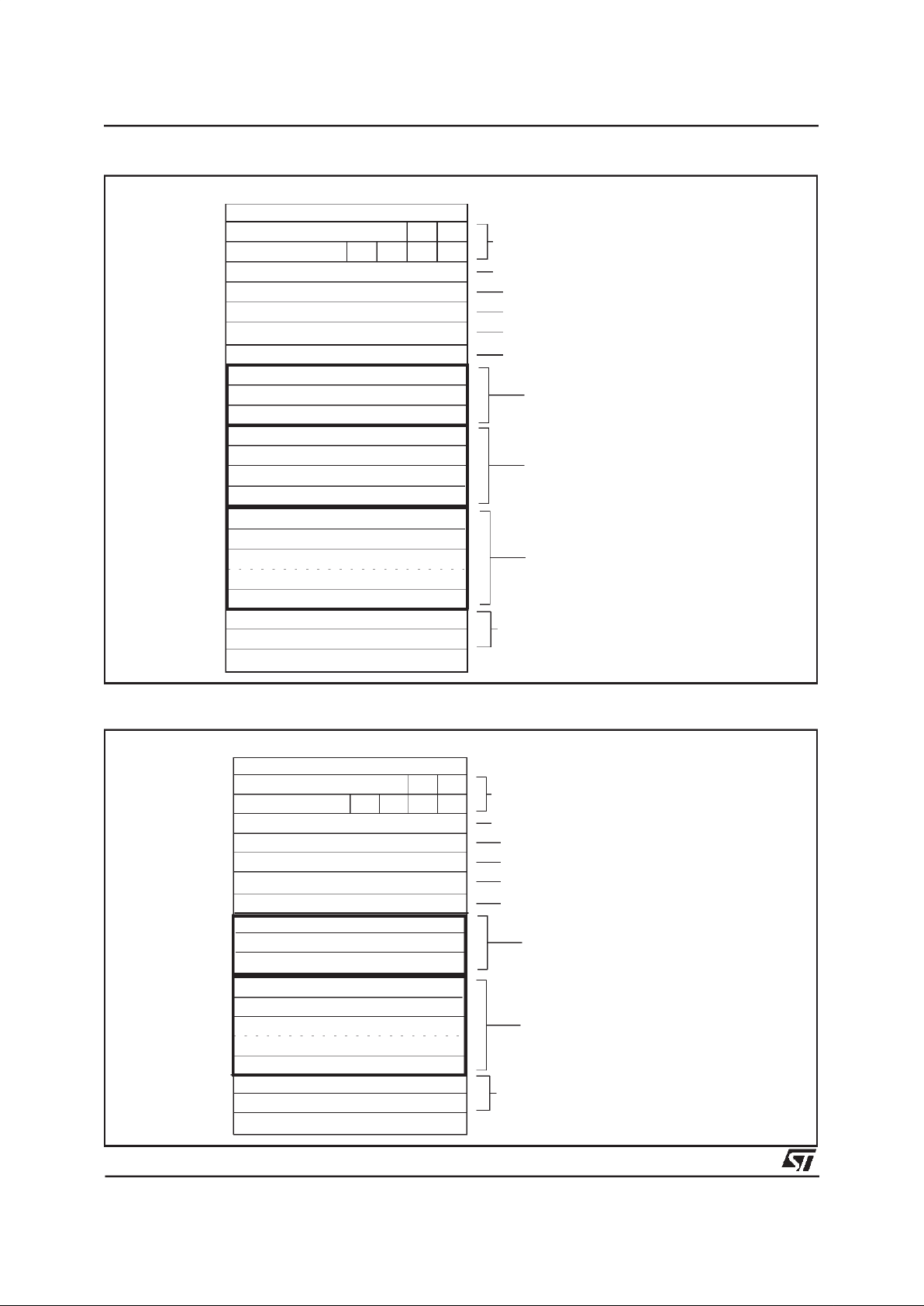
Figure 2: MK50H28SimplifiedBlock Diagram
MK50H28
8/64

3.1 FunctionalBlocks
Refer tothe blockdiagram in Figure2.
The MK50H28 is primarily initialized and control-
led through six 16-bit Control and Status Registers (CSR0 thru CSR5). The CSR’s are accessed
through two bus addressable ports, the Register
Address Port (RAP), and the Register Data Port
(RDP). The MK50H28 may also generate an interrupt(s) to the Host. These interrupts are enabled and disabled through CSR0.
The on-chip microcontroller is used to control the
movement of parallel receive and transmit data,
and to handle the Addressfield filtering.
3.1.1 Microcontroller
The microcontrollercontrolsall of the otherblocks
of the MK50H28. The microcontroller performs
frame processing and protocol processing. All
primitive processing and generation is also done
here. The microcode ROM contains the control
program of the microcontroller.
3.1.2 Receiver
Serial receive data comes into the Receiver (Figure 2). TheReceiveris responsiblefor:
1. Leadingand trailing flag detection.
2. Deletionof zeroes inserted for transparency.
3. Detectionof idleand abortsequences.
4. Detectionof goodand bad FCS (CRC).
5. MonitoringReceiver FIFO status.
6. Detectionof ReceiverOver-Run.
7. Oddbytedetection.
NOTE: If frames are received that have an odd
number ofbytes thenthe lastbyte of theframe is
said tobe an odd byte.
8. Detectionof non-octetaligned frames.
Such frames are treatedas invalidframes.
3.1.3 Transmitter
The Transmitteris responsiblefor:
1. Serializationof outgoingdata.
2. Generatingand appending the FCS(CRC).
3. Framingthe outgoing frame with flags.
4. Zerobit insertionfor transparency.
5. TransmitterUnder-Run detection.
6. Transmissionof odd byte.
7. RTS/CTScontrol.
3.1.4 Frame Check Sequence or Cyclic RedundancyCheck
The FCS (CRC) on the transmitter or receiver
may be either 16 bit or 32 bit, and is user selectable. For full duplex operation, both the receiver
and transmitter have individual FCS computation
circuits. The characteristicsof the FCSare:
TransmittedPolarity: Inverted
TransmittedOrder: High Order Bit First
Pre-setValue: All 1’s
Polynomial16 bit:
X
16+X12+X5
+1
Remainder16 bit(if receivedcorrectly):
High orderbit-->0001 1101 0000 1111
Polynomial32 bit:
X
32+X26+X23+X22+X16+X12+X11+X10
+
+X
8+X7+X5+X4+X2
+X+1
Remainder32 bit(if receivedcorrectly):
high order bit-->11000111 00000100
11011101 0111 1011
3.1.5 Receive FIFO
The Receive FIFO buffers the data received by
the receiver. This performs two major functions.
First, it resynchronizes the data from the receive
clock to the system clock. Second, it allows the
microcontroller time to finish whatever it may be
doingbefore it has to process the receiveddata.
The receive FIFO holds the data from the receiver
without interrupting the microcontrolleruntil it contains enough data to reach the watermark level.
This watermark level can be programmed in
CSR4 to occur when the FIFO contains at least
18 or more bytes; 34 or more bytes; or 50 or
more bytes. Thisprogrammability, alongwith the
programmableburst length of the DMA controller,
enables the user to define how oftenand for how
long the MK50H28 must use the host bus. For
more information, see Control/StatusRegister 4.
For example, if the watermark level is set at 34
bytes and the burst length is limited to 8 word
transfers at a time, the MK50H28 will request
control of the host bus as soon as 34 bytes are
received and again after every 16 subsequent
bytes.
3.1.6 TransmitFIFO
The Transmit FIFO buffers the data to be transmitted by the MK50H28. This also performs two
major functions. First, it resynchronizesthe data
from the system clock to the transmit clock. Second, it allows the microcontroller and DMA controller to burst read data from the host’s memory
buffers; making both the MK50H28 and the host
bus more efficient.
MK50H28
9/64

3.1.7 DMA Controller
The MK50H28has an on-chip DMA Controllercircuit. This allows it to access memory without requiring host software intervention. Whenever the
MK50H28 requires access to the host memory it
will negotiate for mastership of the bus. Upon
gaining controlof the bus theMK50H28 willbegin
transferring data to or from memory. The
MK50H28 will perform memory transfers until
either it has nothing more to transfer, it has
reached its DMA burst limit (user programmable),
or the BUSREL pin is driven low. In any case, it
will complete the current bus transfer before releasing bus mastership back to thehost. If during
a memory transfer, the memory does not respond
within 256 SCLK cycles, the MK50H28 will release ownership of the bus immediately and the
MERR bit will be set in CSR0. The DMA burst
limit can be programmed by the user through
CSR4. In 16 bit mode the limit can be set to 1
word, 8 words, or unlimited word transfers. In 8
bit mode,it can be set to 2 bytes, 16 bytes, or unlimited byte transfers. For high speed data lines
(i.e. > 1 Mbps) a burst limit of 8 words, 16 bytes
or unlimited is suggested to allow maximum
throughput.
The byte ordering of the DMA transfers can be
programmed to accountfor differences in processor architecturesor host programminglanguages.
Byte ordering can be programmed separately for
data and control information. Data information is
defined as all contents of data buffers; control information is defined as anything else in the
shared memory space (i.e. initializationblock, descriptors, etc). For more information see section
4.1.2.5 onControl and StatusRegister 4.
3.1.8 Bus Slave Circuitry
The MK50H28 contains a bank of internal control/status registers (CSR0-5) which can be accessed by the host as a peripheral. The host can
read or write to these registers like any other bus
slave. The contents of theseregistersare listedin
Section 4 and bus signal timing is described in
Figures 13 and 14.
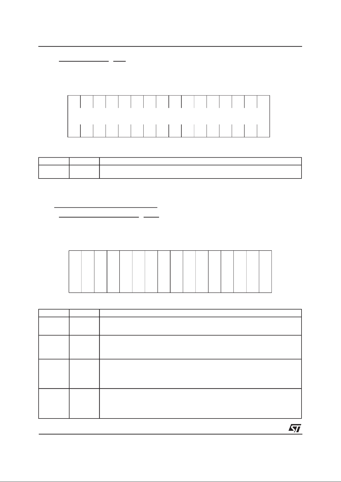
3.2 Memory/Buffer ManagementOverview
The MK50H28 memory structure (Fig. 3) consists
of various blocks of off-chip memory. Only the
Control/Statusregisters,some RAM and firmware
ROM are onboard the chip. The Initialization
Block, Priority DLCI Block, Status Buffer, Address
Lookup Table (ALT), Context Table (CT), Transmit/Receive Rings and Buffers are in the off-chip
memory.
The buffer management is a circular queue of
tasks in memory called descriptor rings. There
are separate rings to describe the transmit and
receive operations. The MK50H28 buffer management mechanism will handle data frames
which are longer than the length of an individual
buffer. This is done by a chaining method which
utilizes multiple buffers. The MK50H28 tests the
next segment in the descriptor ring in a lookahead manner. If the packet is too long for one
buffer, the next buffer will be used after filling the
first buffer (that is chained to the previous buffer).
The MK50H28 will then look ahead to the next
buffer, and chain that buffer also if necessary,
and so on.
3.2.1 InitializationBlock
The MK50H28 initialization information is located
in a block of off- chip memory called the Initialization Block. The Initialization Block consists of 44
contiguous words of memory starting on a word
boundary. The starting address for the initialization block, IADR, is defined in the CSR2 and
CSR3 registers inside the MK50H28. This memory is assembled by the HOST, and the first 15
words are accessed by the MK50H28 during initialization. The Initialization Block (refer to section 4.2) is comprisedof:
A. Mode of Operation.
B. The nN1, nN2, andnN3 counters.
C. The dN1(MaxFrameLength) counter.
D. The nT1,nT2and TP (Transmit Polling)timers.
E. Pointer to thebeginningof Context Table.
F. PointertothebeginningofAddressLookupTable.
G. Pointer to the beginning of StatusBuffer.
H. Error Countersand Statistics.
3.2.1.1 Priority DLCI Block (PDB)
The Priority DLCI Block consists of ContextTable
indices for the priority channels. These indices
are a mechanism through whichthe host can demand the MK50H28 to immediately service certain desired DLCIs. The host should first set up
entries in the PDB before setting the PTDMD bit
in CSR2. In response to that, the MK50H28, after
completing transmission service of its current
DLCI, will jump to the PDB rather than advancing
to the next entry in the contexttable. Afterservicing all active entries in the PDB, the MK50H28
will return to the Context Table and resume the
transmission service that was in progress before
it was interrupted.
3.2.1.2 InterruptDescriptorRings
The MK50H28 has two descriptor ring structures
for the purpose of queing Transmit and Receive
interrupts. The pointers to these two descriptor
rings are located at IADR+24 thru IADR+30 in the
initialization Block. These descriptor rings are of
MK50H28
10/64

a fixed size of 128 entries each. Each entry will
consist of two 16-bit words containing the24-bit
address of the context table entry (XCTADR or
RCTADR) corresponding to the interrupt, a 7-bit
field for the descriptor index (CURXD or CURRD)
into the associated descriptor ring, and a bit
SRVC which is used to indicate whether the interrupt has been serviced. The SRVC bit is set by
the MK50H28when it writes an interruptto the interrupt ring, and it should be cleared by the host
when it services the interrupt. If the MK50H28 attempts to write an interrupt to the interrupt descriptor ring and finds that SRVC is not clear then
it will issue a Provider Primitive 7 to indicate an
Interrupt Ring MISS (with PPARM=0 to indicate a
Receive Interrupt Ring MISS or PPARM=1to indicate a Transmit Interrupt Ring MISS).
3.2.2 AddressLookup Table(ALT)
The ALT contains the maximum of 1024 or 8192
addresses formed by the Data Link Connection
Identifier (DLCI). The MK50H28can support upto
4 octets of address field. The ALT is used to identify which of the 1024 or 8192 addresses are active. For each active channel it has an Index to
the Context Table(CT). The ALT is only used by
the receive processof the MK50H28.
3.2.3 Context Table(CT)
The MK50H28 performs multi-tasking by means
of a Context Table. Each entry in this table contains all the information relevant to one DLCI
channel. Associated with each DLCI are a set of
descriptor rings that are used for transmittingand
receiving frames. All channel entries, except the
LMI Channel,, have equal priority. The MK50H28
scans each entry in the CT sequentially, or
through the use of an index pointer mechanism,
for any available frames to be transmitted. When
a User Primitive 8 with UPARM=2 is issued to the
MK50H28. polling of the LMI/LIV channel will be
enabled to occur between each poll of the other
CT entries.
3.2.4 TransmitDescriptor Ring(s)
The transmit descriptor ring is a circular queue of
tasks that point to data buffers.A variable number
of buffers may be queued-upon a descriptorring
awaiting execution by the MK50H28. The descriptor ring has a segment assigned to each
buffer. Each segment holds a pointer for the
starting address of the buffer, and holds values
for the length of the buffer and the length of the
frame to be transmitted. Each segmentalso contains an OWNA control bit to denote whether the
MK50H28, or the HOST ”owns” the buffer. For
transmit,when the MK50H28 owns the buffer, the
MK50H28 is allowed and commandedto transmit
the contents of the buffer. When the MK50H28
does not own the buffer, it will not transmit the
data in that buffer.
3.2.5 Receive Descriptor Ring(s)
The receive descriptor ring is circular queue of
tasksthat point todata buffers.A variablenumber
of buffers may be queued-upon a descriptor ring
awaiting execution by the MK50H28. The descriptor ring has a segment assigned to each
buffer. Each segment holds a pointer for the
starting address of the buffer, and holds values
for the length of the buffer and the length of the
frame received. Each segment also contains an
OWNA control bit to denote whether the
MK50H28, or the HOST ”owns” the buffer. For
receive, when the MK50H28 owns the buffer, the
MK50H28 may place received data into that buffer. Conversely, when the MK50H28 does not
own a receive buffer, it will not place received
data in that buffer.
3.2.6 Frame Format
The frame format supported by the MK50H28 is
shown below. Each frame may consist of a programmable number of leading flag patterns
(01111110),an address field, an information field,
an FCS (CRC) of either 16 or 32 bits, and a trailing flag pattern. The number of leading flags
transmitted is programmable through the Mode
Registerin the InitializationBlock. The MK50H28
is capable of transmitting and receiving a single
flag between adjacentframes.
TRANSMITTED FIRST
3.2.7 MK50H28 Supported Frame Types
The MK50H28 supports all frame types shown in
Table 1. In LMI, both User and Network Modes
of operation, along with ”Optional Bidirectional
Network Procedures” (Annex D, ANSI T1.617 -
1991)are supported.
ADDRESS INFO FLAG
16/24/32
8*n
8
FLAG
FCS
8 16/32
MK50H28
11/64
INIT BLOCK
PTR TO INIT
MODE
PTR TO ALT
PTR TO STATUS
PTR TO CT
ADDRESS
LOOKUP
TABLE
RING0XMIT
BUFF
0
BUFF ADDRESS
BUFF SIZE
BUFF MSG CNT
DESC 0
TIMER VALUES
ACT. CHNL
(1 ENTRY/ACT. CHNL)
BUFFERS
DATA
ACTIVE CHNL. 1
ACTIVE CHNL. N
TABLECONTEXT
RING NXMIT
BUFF SIZE
BUFF MSG CNT
DESC 0
DESC 1
DESC M
BUFF
M
DESC 1
DESC N
BUFF ADDRESS
BUFF
1
BUFF
1
BUFF
N
LMI ERROR
STATUS
BUFFER
CSR2, CSR3
COUNTERS
BUFF
0
RX RING N
DESC 0
DESC 1
BUFF
0
BUFF
Y
DESC Y
BUFFERS
DATA
BUFF ADDRESS
BUFF SIZE
BUFF MSG CNT
BUFF
1
RX RING 0
DESC 0
DESC 1
BUFF
0
BUFF
X
DESC X
BUFFERS
DATA
BUFF ADDRESS
BUFF SIZE
BUFF MSG CNT
BUFF
1
DESC RING PTRS
ACTIVE CHNL. 0
CONG STATISTICS
DLCI /ADDRESS
CONG STATISTICS
DLCI / ADDRESS
DESC RING PTRS
CONG STATISTICS
DLCI / ADDRESS
DESC RING PTRS
BUFFER
(DLCI 0
to
DLCI 1024
PRIORITY DLCI
BLOCK
or
DLCI 8192)
RX INTERRUPT RING
DESC 0
DESC 1
DESC 127
RX CT Address
Current RX Desc
Service Bit
TX INTERRUPT RING
DESC 0
DESC 1
DESC 127
TX CT Address
Current TX Desc
Service Bit
PTR TO TINT DR
PTR TO RINT DR
Figure 3: MK50H28Memory Management Structure
MK50H28
12/64

3.2.8 Modes of ProtocolOperation
The User modeof operation is entered by issuing
an Auto LMI primitive 7 with UPARM=0. In this
mode, the device transmits STATUS ENQUIRY
messages to the network with an interval determined by the nT1timer. After every nN1 transmissions of STATUS ENQUIRY with Report Type of
”Length Integrity Verification (LIV) Only” the
MK50H28 transmits a STATUS ENQUIRY with
Report Type of ”FullStatus”.
When a STATUS frame is received in response to
a STATUS ENQUIRY(LIV only), the receive sequence number received from the Network side
is checked against the User send sequence number. A received Full STATUS frame will be stored
into the LMI/LIV channel buffer, the sequence
number checkingwill be performed,and its reception will be indicated to the host via Provider
Primitive 13. An availabletransmit or receive buffer is not required for the MK50H28 automatic
processingof ”LIVonly” frames.
A received Asynchronous STATUS frame will be
stored into the LMI/LIV channel buffer and its reception will be indicated to the host via Provider
Primitive 14. If a STATUS ENQUIRY frame (Full
or LIV only) is received in this mode of operation,
the MK50H28 will discard the frame and increment the Discarded Frames Counter in Context
Table enrtry 0. Also see nT1 description in 4.2.2
Timer/Countersection.
The Network mode of operation is enteredby is-
suing an Auto LMI primitive 7 with UPARM=1. In
this mode, the device automatically responds to
STATUS ENQUIRY with Report Type of ”Length
Integrity Verification (LIV) Only” by transmitting a
STATUS frame with Report Type of ”LIV Only”
along with restarting the nT2 timer. An available
transmit or receive buffer is not required for the
MK50H28 automatic processing of ”LIV only”
frames.
When a STATUS ENQUIRY with Report Type of
”Full Status” is received, the device issues the
LMI Received primitive 13 (with PPARM=1) and
expects the host to respond with an LMI Status
Request Primitive 11 with UPARM=0 (when the
host is readyto transmitthe Full STATUSframe).
Asynchronous STATUS frames may be transmitted by placing the data to be transmitted into the
appropriate buffer and issueing Primtive 11 with
UPARM=2. If a STATUS frame(Full,LIV Only,or
Asynchronous)is received in this mode of operation, the MK50H28 will discard the frame and increment the Discarded Frames Counter in Context Table enrtry 0. Also see nT2 description in
4.2.2Timer/Countersection.
The Bi-directional Network Procedures mode
is entered by issuing an Auto LMI primitive 7 with
UPARM=2. The MK50H28 supports this operation using separate User and Network sequence
numbers and N392 and N393 counters. In this
mode, the device transmits STATUS ENQUIRY
messages with a User set of sequence numbers
at an interval determined by the nT1/T391 timer.
The expected response is a STATUS frame with
corresponding sequence numbers. After every
nN1/N391 transmissions of STATUS ENQUIRY
with Report Type of ”LIV Only”, the MK50H28
transmits a STATUS ENQUIRY with Report Type
of ”Full Status”.
A received Full STATUS frame will be stored into
the LMI/LIV channel buffer, the sequence number
checking will be performed, and its reception will
be indicated to the host via Provider Primitive 13.
A received Asynchronous STATUS frame will be
stored into the LMI/LIV channel buffer and its reception will be indicated to the host via Provider
Primitive 14.
In this mode, the device also automatically responds to STATUS ENQUIRY (”LIV Only”) by
transmitting a STATUS (”LIV Only”) frame along
with restarting the nT2 timer.Whena ”Full Status”
Table 1 - MK50H28Frame Types
INFORMATION ELEMENT NAME DIRECTION
Message Type Encoding
MSB LSB
Message Type STATUS_ENQUIRY User -> Network 0 1 1 1 0 1 0 1
STATUS Network -> User 0 1 1 1 1 1 0 1
UPDATE_STATUS Network <-> User 0 1 1 1 1 0 1 1
NOTES:
1. STATUS_ENQUIRY Frame - This Frame has the format as shown inFigure 4.
2. STATUS Frame - This Frame has the format as shownin Figure 5. If Full STATUS information is to be sent, the
host must specify the PVC_STATUS Information Element(s) in thetransmit buffer(s).
3. Asynchronous STATUS Frame - This Frame has the format as shownin Figure 6.The host must specify the PVC_
STATUS Information Elementin the transmit buffer(s).
4. UPDATE_STATUS Frame - Not used in most current applications, MK50H28 supported for backwards compatibility.
MK50H28
13/64

STATUS ENQUIRY is received, the device issues the LMI Received primitive 13 (with
PPARM=1) and expects the host to respondwith
LMI Status Request Primitive 11 with UPARM=0
(when the host is ready to transmit the Full
STATUSframe).
Asynchronous STATUS frames may be transmitted by placing the data to be transmitted into the
appropriate buffer and issueing Primtive 11 with
UPARM=2.
LMI frames received in any mode will not cause
Receive Interrupts (RINT) to be generated, nor
will the Receive Interrupt Ring be updated. Instead, the MK50H28 will issue primitives corresponding to those LMI Frame received which are
not automaticallyprocessedby the MK50H28(i.e.
non ”LIV only” frames). See the description of
primitives in section 4.1.2.2. In addition to the
primitives, bits09-11 of the Receive MessageDescriptor0 (RMD0)for theLMI channelwill indicate
the type of frame received. See section 4.3.1.2
for details.
In Non-Auto-LMI mode of operation, LMI frames
received on the LMI Channel (typically DLCI 0)
will be writteninto the receive buffer as Transparent or SVC frames.
Also refer to DetailedProgramming Procedures
(section 4.4) for more information on using the
devicein thepreviously mentioned modes of ProtocolOperation.
MK50H28
14/64

11111100
11110001
01111110
01010001
1
00000000
01010011
2
CURRENT SEQ
LAST RCVD SEQ
MANAGEMENT DLCI
UN-NUMBERED INFO FRAME
PROTOCOL DISCRIMINATOR
CALL REFERENCE (null)
STATUS MESSAGE
REPORT_TYPE IE
(Full STATUSMessage)
Link Integrity Verification IE
87654321
FCS (msb)
FCS (lsb)
01111110
FRAME FCS
00000011
00001000
00000000
01111101
01010111
3
PVC DLCI (msb)
PVC DLCI (lsb)
PVC_STATUS IE
00
1
0
00
1000N0A0
Figure 5: SampleAnnexA STATUSFrame (Full)
11111100
11110001
01111110
00000011
00001000
00000000
01110101
01010001
1
00000001
01010011
2
CURRENT SEQ
LAST RCVD SEQ
FCS (msb)
FCS (lsb)
01111110
MANAGEMENT DLCI
UN-NUMBERED INFO FRAME
PROTOCOL DISCRIMINATOR
CALL REFERENCE(null)
STATUS_ENQUIRY MESSAGE
REPORT_TYPE IE
(Requesting a LIV Only
STATUS Message)
Link Integrity Verification IE
FRAME FCS
87654321
Figure 4: SampleAnnexA STATUS_ENQUIRYFrame
MK50H28
15/64
11111100
11110001
01111110
00000001
1
00000010
MANAGEMENT DLCI
UN-NUMBERED INFO FRAME
PROTOCOL DISCRIMINATOR
CALL REFERENCE (null)
STATUS MESSAGE
REPORT_TYPEIE
(AsynchronousSTATUS Message)
87654321
00000011
00001000
00000000
01111101
FCS (msb)
FCS (lsb)
01111110
FRAME FCS
00000111
1000N0A0
3
PVC DLCI (msb)
PVC DLCI (lsb)
PVC_STATUSIE
10010101
LOCKING SHIFT(ANSI Annex D Only)
1
00
000
Figure 7: SampleAsynchronousSTATUS Frame (AnnexD)
11111100
11110001
01111110
00000001
1
00000000
00000011
2
CURRENT SEQ
LAST RCVD SEQ
MANAGEMENT DLCI
UN-NUMBERED INFO FRAME
PROTOCOL DISCRIMINATOR
CALL REFERENCE (null)
STATUS MESSAGE
REPORT_TYPEIE
(Full STATUS Message)
LengthIntegrity VerificationIE
87654321
00000011
00001000
00000000
01111101
FCS (msb)
FCS (lsb)
01111110
FRAME FCS
00000111
1000N0A0
3
PVC DLCI (msb)
PVC DLCI (lsb)
PVC_STATUSIE
10010101
LOCKING SHIFT(ANSI Annex D Only)
1
00
000
Figure 6: SampleAnnexD STATUSFrame (Full)
MK50H28
16/64

SECTION4
PROGRAMMINGSPECIFICATION
This section defines the Control and Status Registers and the memory data structures required to
program the MK50H28.
4.1 Control and StatusRegisters
There are six Control and Status Registers
(CSR’s) resident within the MK50H28. The
CSR’s are accessed through two bus addressable ports, an address port (RAP), and a data
port (RDP), thus requiring only two locations in
the system memoryor I/Omap.
4.1.1 Accessing the Contro l and Status Regi sters
The CSR’s are read (or written) in a two step operation.The address of theCSR is writteninto the
address port (RAP) during a bus slave transaction. During a subsequentbus slave transaction,
the data being read from (or written into) the data
port (RDP) is read from (or written into) the CSR
selected in the RAP. Once written, the address in
RAP remains unchanged until rewritten or upon a
bus reset. A control I/O pin (ADR) is providedto
distinguishthe address port fromthe data port.
ADR Port
4.1.1.1 Register AddressPort (RAP)
00000000
B
M
8
000
CSR
<2:0>
15141
3
0
7
0
8
1
0
1
1
1
2
0
1
0
2
0
3
0
4
0
5
0
0
0
9
0
6
H
B
Y
E
T
BIT NAME DESCRIPTION
15:08 RESERVED Must be written as zeroes
07 BM8 When set, places chip into 8 bit mode. CSR’s, Init Block, and data transfers are all 8 bit
transfers; this provides compatibility with 8 bitmicroprocessors. When clear, all transfers
are 16 bit transfers. This bitmust be set to the same valueeach time it is written,
changing this bitduring normal operation will achieve unexpectedresults. BM8 is
READ/WRITE and cleared on Bus RESET.
06:04 RESERVED Must be written as zeroes
03:01 CS3<2:0> CSR address select bits. READ/WRITE. Selects the CSR to be accessed through the
RDP. RAP is cleared by Bus RESET.
CSR<2:0> CSR
0 CSR0
1 CSR1
2 CSR2
3 CSR3
4 CSR4
5 CSR5
00 HBYTE Determines which byte isaddressed for 8 bit mode. If set,the high byte of the register
referred to by CSR<2:0> is addressed, otherwisethe low byte is addressed. This bit is
only meaningfulin 8 bit mode and must be written as zero if BM8=0.HBYTE is
READ/WRITE and cleared on bus reset.
MK50H28
17/64
CSR DATA
1
5
1
0
1
4
0
9
121
1
0
8
0
3
0
7
0
2
06050
4
010
0
1
3
4.1.1.2 Register Data Port (RDP)
BIT NAME DESCRIPTION
15:00 CSR DATA Writing data to theRDP loads data into the CSR selected by RAP. Reading thedata from
RDP reads the data from the CSR selected in RAP.
15141
3
0
7
0
8
1
0
1
1
1
2
0
1
0
2
0
3
0
4
0
5
0
0
0
9
0
6
0
R
I
N
T
T
I
N
T
P
I
N
T
T
U
R
M
I
S
S
M
E
R
R
R
O
R
I
N
T
R
R
X
O
N
T
X
O
N
I
N
E
A
S
T
O
P
D
T
X
D
R
X
P
T
D
M
D
4.1.2 Control and Status Register Definition
4.1.2.1 Controland Status Register 0 (CSR0)
RAP<3:1> = 0
BIT NAME DESCRIPTION
15 PTDMD Transmit Demand for PriorityDLCIs. Setting this bit to1 causes the MK50H28 tojump to
Priority DLCI Block (PDB).This bit is cleared by the MK50H28 after servicing allactive
entries in the PDB. (Note: See section4.2.9 for moredetails.)
14 STOP STOP, when set,indicates that MK50H28 is operating in the STOPPED Phase of
operation. All external activity is disabled and internal logic is reset. MK50H28 remains
inactive except for primitive processinguntil a START primitive is issued. STOP IS READ
ONLY andset by BusRESET or a STOP primitive. Writing to this bit has no effect.
13 DTX Disable Transmitter. Prevents the MK50H28 from further access to the Transmitter
Descriptor Rings. No transmissionsare attempted after finishingtransmission of any
frame intransmission at the time of DTX beingset. Even LMI frames normallygenerated
automatically will not be transmitted if DTX=1. TXON acknowledges changes to DTX,
see below. DTX is READ/WRITE.
12 DRX Disable the Receiver prevents the MK50H28 from further access to the Receiver
Descriptor Rings. No received frames areaccepted afterfinishing reception of any frame
in receptionat the time of DRX being set. Setting DRX will put theMK50H28 in the
LOCAL BUSY Phase. RXON acknowledges changesto DRX, see description of RXON.
DRX is READ/WRITE.
MK50H28
18/64

BIT NAME DESCRIPTION
11 TXON TRANSMITTER ON indicates that the transmit ring access is enabled.TXON is set as
the Startprimitive is issued if the DTX bit is”0” orafterward as DTX is cleared. TXON is
cleared upon recognition of DTX being set, by sending a Stop primitive in CSR1, or by a
Bus RESET. If TXON is clear, the host may modify the Transmit Descriptor Rings entries
regardless of the state of the OWNA bits. TXON is READ ONLY; writing to this bit has no
effect.
10 RXON RECEIVER ON indicates that the receive ring access is enabled. RXON is setas the
Start primitive is issued ifthe DRXbit is”0” or afterwardas DRX is cleared. RXON is
cleared upon recognition of DRX being set, by sending a Stopprimitive in CSR1, or by a
Bus RESET. RXON is READ ONLY; writing to this bit has no effect.
09 INEA INTERRUPT ENABLE allows the INTR I/O pin to be driven low when the Interrupt Flag
is set.If INEA = 1 and INTR = 1 the INTR I/O pin will be low.If INEA = 0 the INTR I/O
pin will be high, regardless of the state of the Interrupt Flag (TINT, RINT, or PINT) or
whether the Interrupt Desciptor Ring has been updated. INEA is READ/WRITE set by
writing a ”1” into thisbit and is cleared by writing a ”0” into this bit, byBus RESET, or by
issuing a Stop primitive. INEA may not be set while in the STOPPED Phase.
08 INTR INTERRUPT FLAG indicatesthat one ormore ofthe followinginterrupt causing
conditions has occurred: MISS, MERR, RINT, TINT, PINT. If INEA = 1 and INTR = 1 the
INTR I/Opin willbe low. INTR is READ ONLY, writing this bit has no effect. INTR is
cleared as the specificinterrupting condition bits are cleared. INTR is alsocleared by
Bus RESETor by issuing a Stopprimitive.
07 MERR MEMORY ERROR is set whenthe MK50H28is the Bus Master and READYhas not
been asserted within 256 SYSCLKs (25.6 usec @ 10MHz) after asserting the address on
the DALlines. When a Memory Error is detected, the MK50H28 releases the bus,
the receiverand transmitter areturned off, and an interrupt is generated if INEA = 1.
MERR is READ/CLEAR ONLY and isset by the chipand cleared by writing a ”1” intothe
bit. Writinga ”0”has no effect. It is cleared by Bus RESET or by issuing a Stop primitive.
06 MISS MISSED frame is set when the receiving channel loses a frame because it is either not
ready or does not own a receive buffer indicating loss of data. The Memory Address for
which MISS occurred can be determined by issuing a Status Request primitive (see
section 4.3.3 Status Buffer for additional details). When MISS is set, an interrupt will be
generated if INEA = 1. MISS is READ/CLEAR ONLY and is set by MK50H28 and
cleared by writing a ”1” into the bit. Writing a ”0” has no effect. It is also cleared by Bus
RESET or by issuing a Stop primitive.
05 ROR RECEIVER OVERRUN indicates that the Receiver FIFO was full when thereceiver was
ready to input data to the ReceiverFIFO. The frame being received is lost, butis
probably recoverable if an upper level protocol is used. When ROR is set, an interrupt is
generated if INEA=1. ROR is READ/CLEAR ONLY and is set by MK50H28 and
cleared by writing a ”1” into the bit. Writing a ”0” has no effect. It is also cleared by Bus
RESET or by issuing a Stop primitive.
04 TUR TRANSMITTER UNDERRUN indicates that the MK50H28 has aborted a frame since
data was late from memory. This condition is reached when the transmitter and
transmitter FIFO both become empty while transmitting a frame. WhenTUR isset, an
interrupt is generated if INEA = 1. TUR is READ/CLEAR ONLY and isset by MK50H28
and clearedby writing a ”1” into the bit. Writinga ”0” has no effect. It is also cleared by
Bus RESETor by issuing a Stopprimitive.
03 PINT PRIMITIVE INTERRUPT is set after the chip updates the primitive register to issue a
provider primitive. When PINT isset, an interruptis generatedif INEA =1. PINT is
READ/CLEAR ONLY and isset by MK50H28 and cleared by writing a ”1” into the bit.
Writing a ”0” has no effect. It is also clearedby Bus RESETor by issuing a Stop primitive.
02 TINT TRANSMITTER INTERRUPT is set after the chip updates an entry in theTransmit
Descriptor Ring.When TINT is set,an interrupt is generated if INEA = 1. TINT is
READ/CLEAR ONLY and isset by the MK50H28 and cleared by writing a ”1” into the bit.
Writing a ”0” has no effect. It is also clearedby Bus RESETor by issuing a Stop primitive.
01 RINT RECEIVER INTERRUPT is set after the MK50H28 updates an entry in the Receive
Descriptor Ring (this is done once per received frame, not per receivedbuffer). When
RINT is set, aninterrupt is generated if INEA = 1. RINT is READ/CLEAR ONLY and is
set by theMK50H28 and clearedby writing a ”1” into the bit. Writing a ”0” hasno effect.
It iscleared by Bus RESET or by issuing a Stop primitive.
00 0 This bit is READ ONLY and will always read as zero.
MK50H28
19/64

1
5
1
0
1
4
0
9
121
1
0
8
0
3
0
7
0
2
06050
4
010
0
1
3
UPRIM
< 3:0 >
PPRIM
< 3:0 >
U
E
R
R
U
A
V
P
A
V
P
L
O
S
T
U
P
A
R
M
:
P
P
A
R
M
1
0
:
1
0
4.1.2.2 Controland Status Register 1 (CSR1)
RAP <3:1> = 133/
BIT NAME DESCRIPTION
15 UERR USER PRIMITIVE ERROR isset by the MK50H28 when a primitive is issued by the
user which is in conflictwith thecurrent status of the chip. UERR is READ/CLEAR
ONLY andis set by MK50H28 and cleared by writing a ”1” into the bit. Writing a ”0” in
this bit has no effect. It is also cleared by Bus RESET.
14 UAV USER PRIMITIVE AVAILABLE is set by the user when a primitive is written into UPRIM.
It iscleared by the MK50H28 after the primitive has been processed. This bit is also
cleared by a BusRESET.
13:12 UPARM USER PARAMETER is written by the host inconjunction with the user primitives in
UPRIM. This User Parameter fieldprovides information to the MK50H28 concerning the
corresponding user primitive. NOTE: For all primitives UPARM = 0 unless otherwise
indicated.
11:08 UPRIM USER PRIMITIVE is written by the user,in conjunction with setting UAV, to control the
MK50H28 linkprocedures. The following primitives are available:
0 Stop: Causes MK50H28 to enter the STOPPED Phase. All link activity is terminated
and theSTOP bit is set. All DMA activity ceases. The transmitter outputs all ones, and all
received data is ignored.
1 Start: Instructs the MK50H28 to exit theSTOPPED Phase and enter the INFORMATION
TRANSFER Phase. The Context Table and the Descriptor Rings are Reset. The
transmitter begins to output flags. The Start primitive isvalid only after the deviceis
initialized (Init Request performed.) If the Auto LMI primitive isnot issued after a Start
primitive, then the only way to transmit LMI frames is through the use of LMI
primitives (10, 11, 12, & 14), and processing is performed on received LMI frames,
but no automatic response or action is taken. Valid onlyin STOPPED phase.
2 Init Request: Instructs the MK50H28 toread the InitializationBlock frommemory. This
should be performed prior to the Start primitive or Transparent primitive after a bus reset
or power-up. Valid only in STOPPED phase.
3 Transparent Mode: Instructs the device to exit the STOPPEDPhase, enter the
TRANSPARENT Phase, and resetthe Context Table and Descriptor Rings. No header
stripping or pre-pending is done for any DLCI channel,and noautomatic LMI processing
is possibleinthis mode. All frames are received to Context Table entry 0 associated
descriptor ring and buffers, and the RTAN bit in CT0 should be set so that the entire
received frame will be written to the buffer. Transmission of frames can occur from
any ContextTable entry, including CT0, and theXTRAN bit should be set so that
only the data in the buffer willbe transmitted for the entire frame. This primitiveis only
valid after device Initialization (Init Request performed). Valid only in STOPPED phase.
4 Status Request: Instructs the MK50H28 to write the current chip status intothe
STATUS BUFFER. Valid in all states, but only after the Initprimitive has been previously
issued.
5 Self-Test Request: Instructs the MK50H28 to perform the built in internalself test. Valid
only in the STOPPED Phase. See section 4.4.10 for the self test procedure.
MK50H28
20/64
 Loading...