


SECTION1 - FEATURES
CompleteLevel 2 Implementationof SS7.
Compatible with 1988 CCITT, AT&T, ANSI,
and Bellcore Signalling System Number 7 link
level protocols.
Optional operation to comply with Japanese
TTC JT-Q703specificationrequirements
Pin-for-pin and architecturally compatible with
MK50H25 (X.25/LAPD), MK50H29 (SDLC),
and MK50H28(FrameRelay).
System clock rates up to 33 MHz (MK50H27 -
33), or 25 MHz(MK50H27- 25).
Data rate up to 4 Mbps continuous for SS7
protocol processing, 20 Mbps for transparent
HDLC mode, or up to 51 Mbps bursted
(gapped data clocks,non-continuousdata).
On chip DMA control with programmableburst
length.
DMA transfer rate of upto 13.3Mbytes/sec using optional 5 SYSCLK DMA cycle (150 nS) at
33 MHzSYSCLK.
BufferManagementincludes:
- InitializationBlock
- SeparateReceive and TransmitRings
- VariableDescriptorRing and Window Sizes.
Selectable BEC or PCR retransmission methods, includingforced retransmissionfor PCR.
Handles all 7 SS7 Timers, plus the additional
Signal Unit intervaltimers for JapaneseSS7.
Handles all SS7 frame formatting:
- Zerobit insert and delete
- FCSgenerationand detection
- Framedelimiting with flags
Programmable minimum Signal Unit spacing
(number of flags between SU’s)
Handles all sequencingand link control.
SelectableFCS of 16 or 32 bits.
Testing Facilities:
- InternalLoopback
- SilentLoopback
- OptionalInternalData ClockGeneration
- SelfTest.
Programmablefor fullor half duplex operation
Programmable Watchdog Timers for RCLK
and TCLK(to detect absenceof data clocks)
MK50H27
Signalling System 7
Link Controller
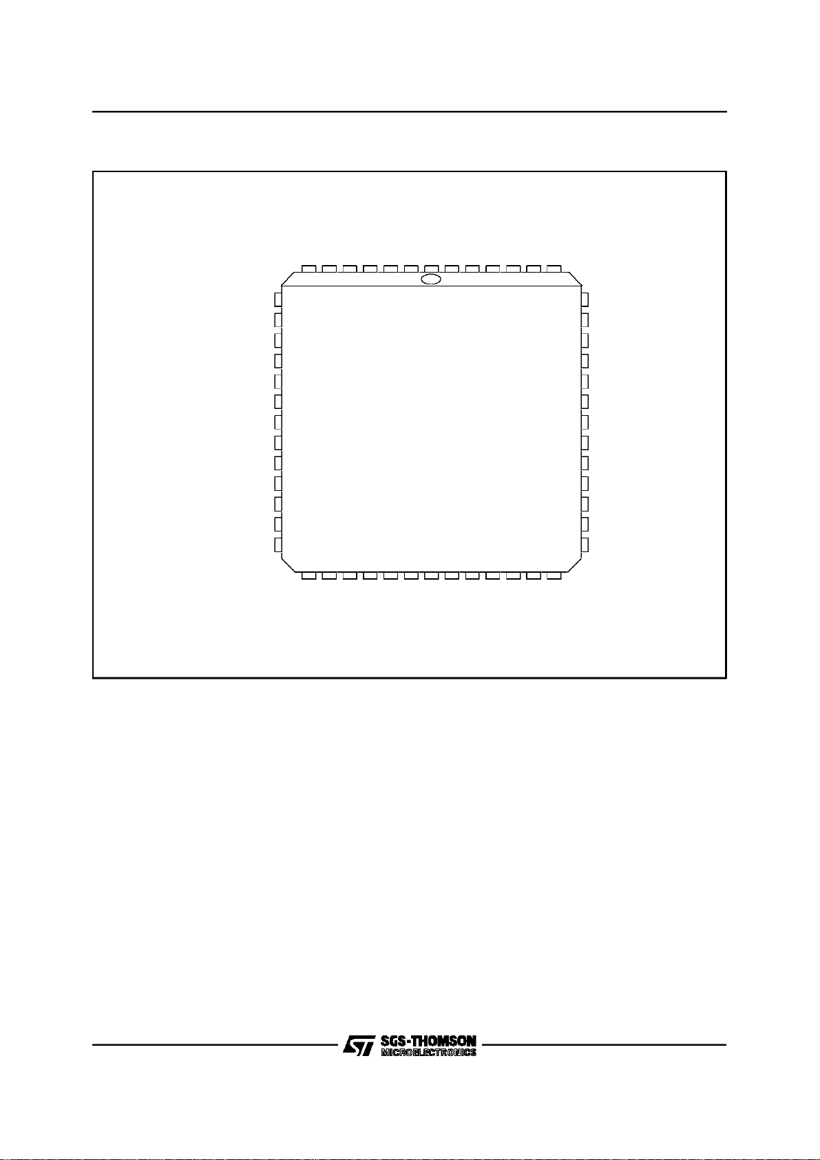
DIP48
PLCC 52
Available in 52 pin PLCC, 84 pin PLCC(for use
with external ROM), or 48pin DIPpackages.
SECTION2 - INTRODUCTION
The SGS - Thomson SS7 SignallingLink Controller (MK50H27) is a VLSI semiconductor device
which provides a complete level 2 datacommunication control conforming to the CCITT, ANSI,
BELLCORE, and AT&T versions of SS7, as well
as options to allow conformance to TTC JT-Q703
(Japanese SS7). This includessignal unit formatting, transparency (so-called ”bit-stuffing”), error
recovery by two types of retransmission, error
monitoring, sequence number control, link status
control,and fill in signal unit generation.
One of the outstanding features of the MK50H27
is its buffer management which includes on-chip
DMA. This feature allows users to handle multiple MSU’s of receive and transmit data at a time.
(A conventionaldata link controlchip plus a separate DMA chip would handle data for only a single
block at a time.) The MK50H27 will move multiple
blocks of receive and transmit data directly into
September 1997
1/56

MK50H27
INTRODUCTION (Continued)
and out of memory through the Host’s bus. A
possible system configurationfor the MK50H27 is
shown in figure 1.
For added flexibility a transparent mode provides
an HDLC transport mechanism without link layer
support. In this mode no protocol processing is
done, all data received between opening flag and
CRC is writtento the sharedmemory buffer and it
is up to the user to take care of the upper level
software.
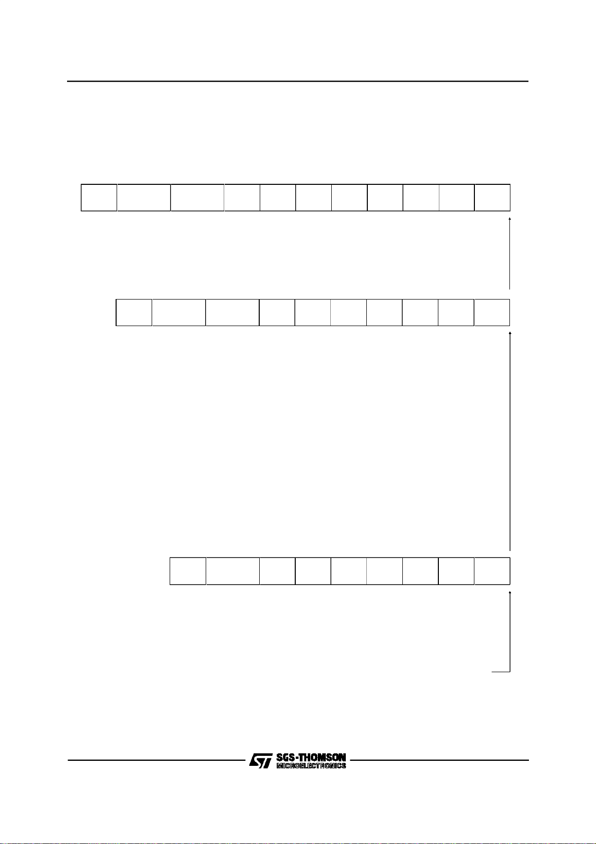
DIP48 PIN CONNECTION (Topview)
VSS-GND
DAL07
DAL06
DAL05
DAL04
DAL03
DAL02
DAL01
DAL00
READ
INTR
DALI
DALO
DAS
BMO, BYTE,BUSREL
BMI, BUSAKO
HOLD, BUSRQ
ALE, AS
HLDA
CS
ADR
READY
RESET
VSS-GND
The MK50H27 may be used with any of several
popular microprocessors, such as: 68040 ...
68000, 6800, Z8000, Z80, 80486 ... 8086, i960,
etc.
The MK50H27 may be operated in either full or
half duplex mode. In half duplex mode, the RTS
and CTSmodem control pins are provided. In full
duplex mode, these pins become user programmable I/O pins. All signal pins on the MK50H27
are TTL compatible. This has the advantage of
makingthe MK50H27independentof the physical
interface. As shown in figure 1, line drivers and
receivers are used for electrical connectionto the
physicallayer.
1
2
3
4
5
6
7
8
9
10
11
12
13
14
15
16
17
18
19
20
21
22
23
24
M
K
5
0
H
2
7
48
47
46
45
44
43
42
41
40
39
38
37
36
35
34
33
32
31
30
29
28
27
26
25
VCC (+5V)
DAL08
DAL09
DAL10
DAL11
DAL12
DAL13
DAL14
DAL15
A16
A17
A18
A19
A20
A21
A22
A23
RD
DSR, CTS
TD
SYSCLK
RCLK
DTR, RTS
TCLK
2/56
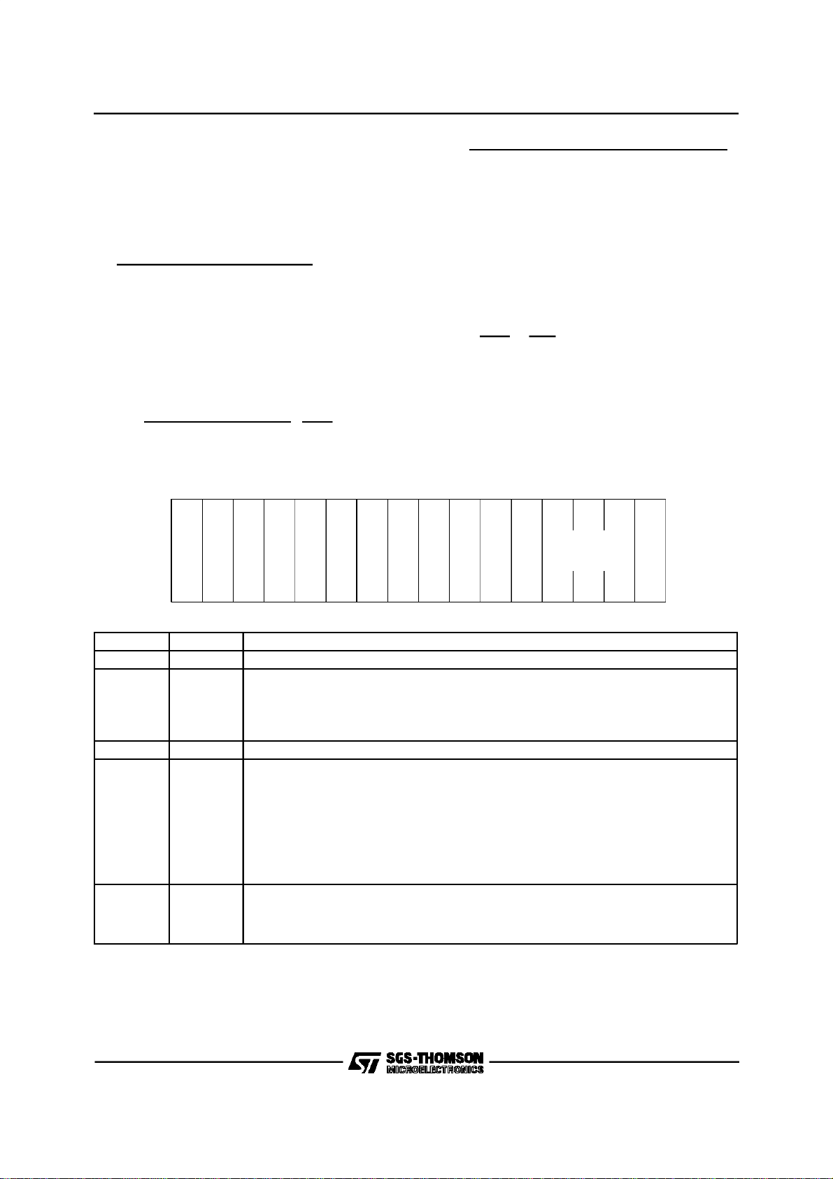
PLCC52 PIN CONNECTION(Top view)
No Connect
7 1 52 47
DAL02
DAL01
DAL00
READ
INTR
DALI
DALO
DAS
BMO/BYTE/BUSREL
No Connect
BM1/BUSAKO
HOLD/BUSRQ
ALE/AS
8
20
21
DAL04
DAL03
DAL05
VCC
VSS
DAL07
DAL06
MK50H27Q
DAL08
DAL09
DAL10
DAL11
33
DAL12
46
34
MK50H27
DAL13
DAL14
DAL15
A16
A17
A18
A19
A20
A21
A22
No Connect
A23
RD
CS
HLDA
ADR
READY
RESET
VSS(GND)
TCLK
No Connect
RCLK
SYSCLK
DTR/RTS
TD
DSR/CTS
3/56

MK50H27
TAble 1 - PIN DESCRIPTION
LEGEND:
I Input only O Outputonly
IO Input/ Output 3S 3-State
OD OpenDrain (no internalpull-up)
Note: Pin out for 52 pin PLCCis shown in brackets.
SIGNAL NAME PIN(S) TYPE DESCRIPTION
DAL<15:00> 2-9
READ 10
INTR 11
DALI 12
DALO 13
DAS 14
BMO
BYTE
BUSREL
BM1
BUSAKO
40-47
[2-10
44-51]
[11]
[12]
[13]
[14]
[15]
15
[16]
16
[18]
IO/3S The time multiplexed Data/Addressbus. During the address portion of a
memory transfer, DAL<15:00> contains the lower16 bits of the memory
address.
During the data portion of a memory transfer, DAL<15:00> contains the read
or write data, depending on the typeof transfer.
IO/3S READ indicatesthe type of operation that thebus controller is performing
during abus transaction. READ is driven by the MK50H27 only while it isthe
BUS MASTER.READ is valid during the entirebus transaction and is
tristated at all other times.
MK50H27 as a BusSlave :
READ = HIGH - Data is placed on the DAL linesby the chip.
READ = LOW - Data is taken off the DAL lines bythe chip.
MK50H27 as a BusMaster :
READ = HIGH - Data is taken off theDAL lines by the chip.
READ = LOW - Data is placed on the DAL lines by the chip.
O/OD INTERRUPT is an attention interrupt line that indicates thatone or more of
the following CSR0 status flags is set: MISS, MERR, RINT, TINT or PINT.
INTERRUPT is enabled by CSR0<09>, INEA=1.
O/3S DALIN is an external bus transceiver control line. DALI is driven by the
MK50H27 only while it is the BUS MASTER. DALI is asserted by the
MK50H27 when it readsfrom the DAL lines during the data portion of a
READ transfer. DALI is not asserted during a WRITE transfer.
O/3S DALOUT is an external bus transceiver control line. DALO is driven by the
MK50H27 only while it is the BUS MASTER. DALO is asserted by the
MK50H27 when it drivesthe DAL linesduring the address portionof a READ
transfer or for the durationof a WRITE transfer.
IO/3S DATA STROBEdefines the dataportion of a bus transaction. By definition,
data is stable and valid at the low to high transition of DAS.Thissignal is
driven by the MK50H27 while it is the BUS MASTER. During the BUS
SLAVE operation, this pin is used as an input. At all other times the signal is
tristated.
IO/3S I/O pins 15 and 16 are programmable through CSR4. If bit 06 of CSR4 is set
to a one, pin 15 becomes input BUSREL and is used by the host to signal
the MK50H27 to terminate a DMA burst after the current bus transferhas
completed. If bit 06 is clear then pin 15 is an outputand behaves as
described belowfor pin 16.
O/3S Pins15 and 16 are programmable through bit 00 of CSR4 (BCON).
If CSR4<00> BCON = 0,
I/O PIN 15 = BMO (O/3S)
I/O PIN 16 = BM1 (O/3S)
BYTE MASK<1:0> Indicates the byte(s) on the DAL to be read or written
during thisbus transaction. MK50H27 drives these lines only as a Bus
Master. MK50H27 ignores the BM lineswhen it is aBus Slave.
Byte selectionis done as outlined in the following table.
BM1 BM0 TYPE OF TRANSFER
LOW LOW ENTIRE WORD
LOW HIGH UPPER BYTE
(DAL<15:08>)
HIGH LOW LOWER BYTE
(DAL<07:00>)
HIGH HIGH NONE
4/56

Table 1: PIN DESCRIPTION(continued)
SIGNAL NAME PIN(S) TYPE DESCRIPTION
HOLD
BUSRQ
ALE
AS
HLDA 19
CS 20
ADR 21
READY 22
17
[19]
18
[20]
[21]
[22]
[23]
[24]
If CSR4<00> BCON = 1,
Byte selectionis done using the BYTE line and DAL<00> latchedduring the
address portion of thebus transaction. MK50H27 drives BYTE onlyas a Bus
Master and ignores it when a Bus Slave. Byte selection is done as outlined
in thefollowing table.
BYTE DAL<00> TYPE OF TRANSFER
LOW LOW ENTIRE WORD
LOW HIGH ILLEGAL CONDITION
HIGH LOW LOWER BYTE
HIGH HIGH UPPER BYTE
BUSAKO is a bus request daisy chainoutput. IfMK50H27 is not requesting
the bus and it receives HLDA, BUSAKO will be driven low. If MK50H27is
requesting the bus when it receives HLDA, BUSAKO will remain high
Note: All transfers are entireword unless the MK50H27 isconfigured for 8 bit
operation.
IO/OD Pin 17 is configured through bit 0 of CSR4.
If CSR4<00> BCON = 0,
HOLD requestis asserted by MK50H27 when it requires a DMA cycle,if
HLDA is inactive, regardless of the previousstate of theHOLD pin. HOLD is
held low for the entireensuing bus transaction.
If CSR4<00> BCON = 1,
BUSRQ is asserted by MK50H27 when it requires a DMA cycle ifthe prior
state ofthe BUSRQ pin was high and HLDA is inactive. BUSRQ is held low
for the entire ensuing bus transaction.
O/3S Theactive level of ADDRESS STROBE is programmable through CSR4.
The address portion of a bustransfer occurs while thissignal is at its
asserted level.This signal is drivenby MK50H27 whileit is the BUS
MASTER. At all other times, the signalis tristated.
If CSR4<01> ACON = 0,
ADDRESS LATCH ENABLE isused to demultiplexthe DAL lines anddefine
the address portion of the transfer. As ALE, the signaltransitions from high
to low during the address portion of the transfer and remains low during the
data portion.
If CSR4<01> ACON = 1,
As AS, the signal pulses low during the address portion of the bus transfer.
The low to hightransition of AS can be used by aslave device to strobe the
address into a register.
AS is effectively the inversion of ALE.
I HOLD ACKNOWLEDGE is theresponse to HOLD. When HLDAis low in
response to MK50H27’s assertion of HOLD, the MK50H27 is the Bus
Master. HLDA should bedeasserted ONLY afterHOLD has been released
by the MK50H27.
I CHIP SELECT indicates, when low, that theMK50H27 is the slave device
for the data transfer. CS must be valid throughout the entire transaction.
I ADDRESS selects the Register Address Port or the Register Data Port. It
must be valid throughout thedata portion of the transfer andis only used by
the chip when CS is low.
ADR PORT
LOW REGISTER DATA PORT
HIGH REGISTER ADDRESS PORT
IO/OD When the MK50H27 is a Bus Master, READY is an asynchronous
acknowledgement from the busmemory thatmemory willaccept data in a
WRITE cycle or thatmemory has put data on the DALlines in a READ cycle.
I/O PIN 15 = BYTE (O/3S)
I/O PIN 16 = BUSAKO (O)
I/O PIN 17 = HOLD
I/O PIN 17 = BUSRQ
I/O PIN 18 = ALE
I/O PIN 18 = AS
MK50H27
5/56

MK50H27
Table 1: PIN DESCRIPTION(continued)
SIGNAL NAME PIN(S) TYPE DESCRIPTION
As a Bus Slave,the MK50H27 asserts READY when it has put data on the
DAL linesduring a READ cycle or is about to take data from the DAL lines
during aWRITE cycle. READY is a response to DAS and it will be released
after DAS or CS is negated.
RESET 23
TCLK 25
DTR
RTS
RCLK 27
SYSCLK 28
TD 29
DSR
CTS
RD 31
A<23:16> 32-39
VSS-GND 1,24
VCC 48
[25]
[28]
26
[29]
[30]
[31]
[32]
30
[33]
[34]
[37-43]
[1,26]
[52]
I RESET is the Bus signal that will cause MK50H27 to cease operation, clear
its internal logic and enter an idle state with the Stop bit ofCSR0 set.
I TRANSMIT CLOCK. A 1x clock input for transmitter timing. TD changes on
the fallingedge of TCLK. The frequency of TCLK may not be greater than
the frequency of SYSCL
IO DATA TERMINAL READY, REQUEST TOSEND. Modem controlpin. Pin
26 is configurable through CSR5. Thispin can be programmed to behave as
output RTS or as programmable IO pin DTR. If configured as RTS, the
MK50H27 will assert this pin if it has data to send and throughout the
transmission of a signal unit.
I RECEIVE CLOCK. A 1x clock input for receiver timing. RD is sampled on
the rising edge ofRCLK. The frequency of RCLK may notbe greater than
the frequency of SYSCLK.
I SYSTEM CLOCK. System clock used for internal timing ofthe MK50H27.
SYSCLK shouldbe a squarewave, of frequency up to 33 MHz.
O TRANSMIT DATA. Transmitserial data output.
IO DATA SET READY, CLEAR TO SEND. Modem Control Pin. Pin 30 is
configurable throughCSR5. This pincan be programmed to behave as input
CTS or as programmable IO pinDSR. If configured as CTS, the MK50H27
will transmit all ones while CTS is high.
I RECEIVE DATA. Received serial data input.
O/3S Address bits<23:16> used inconjunction with DAL<15:00> to produce a 24
bit address. MK50H27 drives these lines only as a Bus Master. A23-A20
may be driven continuously as described in the CSR4<7> BAEbit.
Ground Pins
Power SupplyPin
+5.0 VDC + 5%
SECTION3
OPERATIONALDESCRIPTION
The SGS-Thomson MK50H27 Multi-Logical Link
CommunicationsController deviceis a VLSI product intended for high performance data communication applications requiring SDLC link level control. The MK50H27 will perform all frame
formatting, such as: frame delimiting with flags,
FCS (CRC) generation and detection, and zero
bit insertion and deletion for transparency. The
MK50H27 also handles all supervisory (S) and
unnumbered (U) frames (see Tables A & B). The
MK50H27 also includes a buffer management
mechanismthat allowsthe user to transmit and/or
receive multiple frames for each active channel
or DLCI. Contained in the buffer management is
an on-chipdual channel DMA: one channel for receive andone channelfor transmit.
6/56
The MK50H27 can be used with any popular 16
or 8 bit microprocessor. A possible system configuration for the MK50H27 is shown in Figure 1.
This document assumes that the processorhas a
byte addressablememory organization.
The MK50H27 will move multiple blocks of receive and transmit data directly in and out of
memorythroughthe Host’sbus.
The MK50H27 may be operated in full or half duplex mode. In half duplex mode the RTS and
CTS modem control pins are provided. In full duplex mode, these pins become user programmable I/O pins.
All signal pins on the MK50H27 are TTL compatible. This has the advantage of making the
MK50H27 independent of the physical interface.
As shown in Fig. 1, line drivers and receivers are
used for electrical connection to the physical
layer.

Figure 1: PossibleSystem Configuration for thr MK50H27
HOST PROCESSOR
(68020, i960, Z8000, ETC)
MK50H27
MEMORY
(MULTIPLE
DATA BLOCKS)
DTR, RTS
DSR, CTS
16-BIT DATA BUS INCLUDING
24-BIT ADDRESS AND BUS CONTROL
MK50H27
RCLK
RD
TCLK
TD
LINE DRIVERS
AND RECEIVERS
ELECTRICAL I/O
(SUCH AS RS-232C, RS-423, RS-422)
DATA COMM. CONNECTOR
(SUCH AS RS-449, RS-232C, V.35)
7/56

MK50H27
Figure 2: MK50H27Simplified Block Diagram
DALI
DALO
HLDA
HOLD
ALE, AS
BM0
A <23:16>
DAL <15:00>
BM1
DMA
CONTROLLER
READY
READ
DAS
ADR
CS
CONTROL / STATUS
REGISTERS 0 - 5
DTR, RTS
DSR, CTS
INTR
FIRMWARE
ROM
MICRO
CONTROLLER
TIMERS
SYSCLK
RCLK
RD
INTERNAL BUS
RECEIVER
FIFO
RECEIVER TRANSMITTER
LOOPBACK
TRANSMITTER
FIFO
TEST
VCC
VSS -GND
RESET
TCLK
TD
8/56

MK50H27
3.1 Functional Blocks
Refer tothe blockdiagram in Figure2.
The MK50H27 is primarily initialized and control-
led through six 16-bit Control and Status Registers (CSR0 thru CSR5). The CSR’s are accessed
through two bus addressable ports, the Register
Address Port (RAP), and the Register Data Port
(RDP). The MK50H27 may also generate an interrupt(s) to the Host. These interrupts are enabled and disabled through CSR0.
The on-chip microcontroller is used to control the
movement of parallel receive and transmit data,
and to handle the Addressfield filtering.
3.1.1 Microcontroller
The microcontrollercontrolsall of the otherblocks
of the MK50H27. The microcontroller performs
frame processing and protocol processing. All
primitive processing and generation is also done
here. The microcode ROM contains the control
program of the microcontroller.
3.1.2 Receiver
Serial receive data comes into the Receiver (Fig-
ure 2). TheReceiveris responsiblefor:
1. Leadingand trailing flag detection.
2. Deletionof zeroes inserted for transparency.
3. Detectionof idle and abort sequences.
4. Detectionof good& bad CK (ChecKbit seq.)
5. MonitoringReceiver FIFO status.
6. Detectionof Receiver Over-Run.
7. Odd byte detection.
NOTE: If framesare receivedthathavean odd
numberof bytesthen the last byteof the
frame is saidto be an odd byte.
8. Detectionof non-octetalignedframes.Such
framesare treatedas invalid.
3.1.3 Transmitter
The Transmitteris responsiblefor:
1. Serializationof outgoingdata.
2. Generatingand appendingthe CK (CRC).
3. Framingoutgoing frame with flags.
4. Zerobit insertionfor transparency.
5. TransmitterUnder-Rundetection.
6. Transmissionof odd byte.
7. RTS/CTScontrol.
3.1.4 Check Bit Sequenceor Cyclic
Redundancy Check
The CK (CRC) on the transmitter or receiver may
be either 16 bit or 32 bit, and is user selectable.
For full duplex operation, both the receiver and
transmitter have individual CK computation circuits. Thecharacteristics of the CKare:
TransmittedPolarity: Inverted
TransmittedOrder: High OrderBit First
Pre-setValue: All 1’s
Polynomial16 bit:
16+X12+X5
X
+1
Remainder16 bit (if received correctly):
High order bit-->0001 1101 00001111
Polynomial32 bit:
32+X26+X23+X22+X16+X12+X11+X10
X
8+X7+X5+X4+X2
X
+X+1
Remainder32 bit (if received correctly):
high order bit-->110001110000 0100
1101 1101 0111 1011
3.1.5 ReceiveFIFO
The Receive FIFO buffers the data received by
the receiver. This performs two major functions.
First, it resynchronizes the data from the receive
clock to the system clock. Second, it allows the
microcontroller time to finish whatever it may be
doingbefore it has to process the receiveddata.
The receive FIFO holds the data from the receiver
without interrupting the microcontrollerfor service
until it contains enough data to reach the watermark level, or an end of frame is received. This
watermark level can be programmed in CSR4
(FWM) to occur when the FIFO contains at least
18 or more bytes; 34 or more bytes; or 50 or
more bytes. Thisprogrammability, along with the
programmableburst length of the DMA controller,
enables the user to definehow often and for how
long the MK50H27 must use the host bus. For
more information, see CSR4.
For example, if the watermark level is set at 34
bytes and the burst length is limited to 8 word
transfers at a time, the MK50H27 will request
control of the host bus as soon as 34 bytes are
received and again after every 16 subsequent
bytes.
3.1.6 TransmitFIFO
The Transmit FIFO buffers the data to be trans-
mitted by the MK50H27. This also performs two
major functions. First, it resynchronizesthe data
from the system clock to the transmit clock. Second, it allows the microcontroller and DMA controller to burst read data from the host’s memory
buffers; making both the MK50H27 and the host
bus more efficient.
+
9/56

MK50H27
The transmitFIFO has a watermarkscheme similar to the one described for the receive FIFO
above, and uses the same FWM value selections
in CSR4 for the watermark. Once filled to within
FWM of being full (by DMA from TX buffer in
shared memory), the transmit FIFO will not interrupt the microcontroller until it empties enough to
fall below the watermark level.
3.1.7 DMA Controller
The MK50H27has an on-chip DMA Controllercircuit. This allows it to access memory without requiring host software intervention. Whenever the
MK50H27 requires access to the host memory it
will negotiate for mastership of the bus. Upon
gaining controlof thebus the MK50H27 will begin
transferring data to or from memory. The
MK50H27 will perform memory transfers until
either it has nothing more to transfer, it has
reached its DMA burst limit (user programmable),
or the BUSREL pin is driven low. In any case, it
will complete all bus transfers before releasing
bus mastership back to the host. If during a
memory transfer, the memory does not respond
within 256 SCLK cycles, the MK50H27 will release ownership of the bus immediately and the
MERR bit will be set in CSR0. The DMA burst
limit can be programmed by the user through
CSR4. In 16 bit mode the limit can be set to 1
word, 8 words, or unlimited word transfers. In 8
bit mode,it can be set to 2 bytes,16 bytes, or unlimited byte transfers. For high speed data lines
(i.e. > 1 Mbps) a burst limit of 8 words or 16 bytes
is suggestedto allow maximum throughput.
The byte ordering of the DMA transfers can be
programmed to accountfor differences in processor architecturesor host programminglanguages.
Byte ordering can be programmed separately for
data and control information. Data information is
defined as all contents of data buffers;control information is defined as anything else in the
shared memory space (i.e. initializationblock, descriptors, etc). For more information see section
4.1.2.5 oncontrolstatus register 4.
3.1.8 Bus SlaveCircuitry
The MK50H27 contains a bank of internal control/status registers (CSR0-5) which can be accessed by the host as a peripheral. The host can
read or writeto these registers like any other bus
slave. The contents of these registers are listed
in Section 4 and bus signal timing is described in
Figures 9 and 10.
3.2 Buffer Management Overview
Refer toFig. 3.
10/56
3.2.1 InitalizationBlock
Chip initialization information is located in a block
of memory called the Initialization Block. The InitializationBlock consistsof 200 contiguouswords
of memory starting on a word boundary. This
memory is assembled by the HOST, and is accessed by the MK50H27 during initialization. The
InitializationBlock is comprisedof:
A. Mode of Operation.
B. Counter/Timer Preset Values.
C. Protocol Parameters or Options
D. Location and size of Receive and TransmitDe-
scriptorRings.
E. Optional Transmit Window SIzeValue
F. Locationof StatusBuffer.
G. Optional JT-Q703 SignalUnit IntervalTimer
Values
H. Statisticsand ErrorCounters.
3.2.2 The Circular Queue
The basic organizationof the buffer management
is a circular queue of tasks in memory called descriptor rings. There are separate rings to describe the transmit and receive operations. Up to
128 buffers may be queued-up on a descriptor
ring awaiting execution by the MK50H27. The
descriptor ring has a descriptorassigned to each
buffer. Each descriptor holds a pointer for the
starting address of the buffer, and holds a value
for thelength of thebuffer in bytes.
Each descriptor also contains two control bits
called OWNA and OWNB, which denote whether
the MK50H27, the HOST, or an I/O ACCELERATION PROCESSOR ( if present) ”owns” the buffer. For transmit, when the MK50H27 owns the
buffer, the MK50H27 is allowed and commanded
to transmit the buffer. When the MK50H27 does
not own the buffer, it will not transmitthat buffer.
For receive, when the MK50H27 owns a buffer, it
may place received data into that buffer. Conversely, when the MK50H27 does not own a receive buffer, it will not place received data into
that buffer.
The MK50H27 buffer management mechanism
will handle frames which are longer than the
length of an individual buffer. This is done by a
chaining method which utilizes multiple buffers.
The MK50H27tests the next descriptorin the descriptor ring in a ”look ahead” manner. If the
frame is too long for one buffer, the next buffer
will be used after filling the first buffer; that is,
”chained”. The MK50H27 will then ”look ahead”
to the next buffer, and chain that buffer if necessary, and so on.The operational parameters for
the buffer management are defined by the user in
the initialization block. The parameters defined
include the basic mode of operation, protocol options, the number of entries for the transmitter
and receiver descriptor rings, etc. The starting
address for the Initialization block, IADR, is defined in the CSR2 and CSR3 registers inside the
MK50H27.
3.2.3 SignalUnit Repertoire
The frame format supported by the MK50H27 is
shown in Table A. Each signal unit (SU) may
consist of a programmable number of leadingflag
patterns (01111110), Backward Sequence Number, Backward Indicator Bit, Forward Sequence
Number, Forward Indicator Bit, Lenght Indicator
Field, followed by Signalling Information Octet,
Service Information Field, or Status Field, depending on SU type, and then ended with a CK
(CRC) of either 16 or 32 bits, and a trailing flag
pattern. The number of leading flags transmitted
is programmable through the Mode Register in
the Initialization Block. Received signal units may
have as few as one flag between adjacent signal
units
The symbols and definitions for the signal unit
types handledby the MK50H27 are:
MK50H27
NAME DEFINITION
MSU MessageSignal Unit
LSSU Link Status Signal Unit
FISU Fill In Signal Unit
F Flag Sequence (01111110)
FSN Forward SequenceNumber
BSN Backward Sequence Number
FIB Forward IndicatorBit
BIB Backward Indicator Bit
LI Lenght Indicator
X Reserved - programmed as zeroes
PRI Priority Indication (JT-Q703 only)
SIO Signalling Information Octe
SIF Service Information Field
SF Status Field
CK Check bit Sequence (CRC)
TABLE A - MK50H27Signal Unit Repertoire
11/56
MK50H27
TABLE A - MK50H27Signal Unit Repertoire
Message Signal Unit (MSU)
F CK SIF SIO X LI FIB FSN BIB BSN F
8 16/32 8n,n>=2 8 2 6 1 7 1 7 8
Link Status Signal Unit (LSSU)
FCK
8 16/32
Values for SF:
0 - SIO,
1 - SIN,
2 - SIE,
Fill-in Signal Unit (FISU)
SF X LI FIB FSN BIB BSN F
Out of alignment
Normal alignment
Emergency
FCK
8 16/32
26 17 1 7 88/16
3 - SIOS,
4 - SIPO,
5 - SIB,
X LI FIB FSN BIB BSN F
2 6 171 7 8
Out-of-service
Processor outage
Congestion (Busy)
12/56
Right-most fields are transmitted first

Figure 3: MK50H27MemoryManagement Structure
CSR 2, CSR3
POINTER TO
INITIALIZATIONBLOCK
INITIALIZATIONBLOCK
RECEIVER DESCRIPTOR RINGS
DESCRIPTOR 0
BUFFER STATUS
BUFFER ADDRESS
BUFFER SIZE
BUFFER MSGCOUNT
DESCRIPTOR 1
MK50H27
RECEIVE BUFFER
BUFFER
0
BUFFER
1
MODE
TIMER VALUES
PROTOCOL
PARAMETERS
RX DESCRIPTOR
POINTER
TX DESCRIPTOR
POINTER
STATUS
BUFFER ADDRESS
STATISTIC S
STATUS BUFFER
DESCRIPTOR M
TRANSMIT DESCRIPTOR RINGS
DESCRIPTOR 0
BUFFER STATUS
BUFFER ADDRESS
BUFFER SIZE
BUFFER MSG COUNT
DESCRIPTOR 1
BUFFER
M
TRANSMIT BUFFER
BUFFER
0
BUFFER
1
DESCRIPTOR N
BUFFER
N
13/56
MK50H27
SECTION4
PROGRAMMINGSPECIFICATION
This section defines the Control and Status Registers and the memory data structures required to
program the MK50H27.
4.1 Control and StatusRegisters
There are six Control and Status Registers
(CSR’s) resident within the MK50H27. The
CSR’s are accessed through two bus addressable ports, an address port (RAP), and a data
port (RDP), thus requiring only two locations in
the system memoryor I/O map.
4.1.1.1 Register Address Port (RAP)
15141
1
3
2
1
1
1
0
0
9
00000000
4.1.1 AccessingtheControl& StatusRegisters
The CSR’s are read (or written) in a two step op-
eration.The address of theCSR is written into the
address port (RAP) during a bus slave transaction. During a subsequentbus slave transaction,
the data being read from (or written into) the data
port (RDP) is read from (or written into) the CSR
selected in theRAP. Once written, the address in
RAP remains unchanged until rewritten or upon a
bus reset. A control I/O pin (ADR)is provided to
distinguishthe addressport fromthe data port.
ADR Port
L RegisterData Port (RDP)
H RegisterAddressPort (RAP)
0
0
7
8
0
0
5
6
0
0
3
4
0
0
2
0
1
0
H
B
M
000
8
CSR
<2:0>
B
Y
T
E
BIT NAME DESCRIPTION
15:08 RESERVED Must be written as zeroes
07 BM8 When set, places chip into 8 bit mode. CSR’s, Init Block, and data transfers are all8 bit
06:04 RESERVED Must be written as zeroes
03:01 CS3<2:0> CSR address select bits. READ/WRITE. Selects the CSR to be accessed through the
00 HBYTE Determines which byte is addressed for 8 bit mode. If set,the high byte of the register
14/56
transfers; this provides compatibility with 8 bitmicroprocessors. When clear, all transfers
are 16 bit transfers. This bitmust be setto the same valueeach time it is written,
changing this bitduring normal operation will achieve unexpected results. BM8 is
READ/WRITE and cleared on Bus RESET.
RDP. RAP is cleared by Bus RESET.
CSR<2:0> CSR
0 CSR0
1 CSR1
2 CSR2
3 CSR3
4 CSR4
5 CSR5
referred to by CSR<2:0> is addressed, otherwisethe lowbyte is addressed. This bit is
only meaningfulin 8 bit mode and must be writtenas zero if BM8=0. HBYTE is
READ/WRITE and cleared on bus reset.

4.1.1.2 Register Data Port (RDP)
MK50H27
1
1
5
4
121
1
3
1
0
0
0
06050
0
1
9
8
7
0
0
010
3
4
2
0
CSR DATA
BIT NAME DESCRIPTION
15:00 CSR DATA Writing data to the RDP loads data into the CSR selectedby RAP. Reading the data from
RDP reads the data from the CSR selected in RAP.
4.1.2 Control and StatusRegister Definition
4.1.2.1 Controland Status Register 0 (CSR0)
RAP<3:1> = 0
15141
P
T
O
D
F
M
F
D
1
3
D
T
X
1
2
T
D
X
R
O
X
N
0
0
9
R
I
X
N
O
E
N
A
1
1
0
0
7
8
M
I
E
N
R
T
R
R
0
6
M
I
S
S
0
5
R
O
R
0
0
3
4
P
T
I
U
N
R
T
0
0
2
T
I
N
T
0
1
0
R
I
0
N
T
BIT NAME DESCRIPTION
15 TDMD TRANSMITDEMAND,when set,causesMK50H27 to access the
Transmit Descriptor Ring without waiting for the transmit polltime interval to elapse. TDMDneed not be set to transmit a MSU, it merelyhastens MK50H27’s response to a Transmit Descriptor Ring entry insertion by the host. TDMD is Write With ONE ONLY and cleared by the
microcode after it is used. It may read as a ”1” for a shorttime after it
is written because the microcode may have been busy when TDMD
was set. It is also cleared by Bus RESET. Writing a ”0” in this bit has
no effect.
14 POFF POFF,when set, indicates thatMK50H27is operatingin the PowerOff
phase of operation. All external activity is disabled and internal logic is
reset. MK50H27 remains inactive except for primitive processing until
a Power On primitive is issued. POFF IS READONLY and set by Bus
RESETor a PowerOff primitive. Writing to this bithas no effect.
13 DTX Transmitterring disable preventsthe MK50H27from furtheraccess to
the Transmitter Descriptor Ring and terminates transmitter polling. No
transmissions are attempted after finishing transmission of any signal
unit in transmission at the time of DTX being set. TXON acknowledgeschanges to DTX, see below. DTX is READ/WRITE.
15/56

MK50H27
4.1.2.1 Controland Status Register 0 (CSR0)
BIT NAME DESCRIPTION
12 DRX Disablethe Receiverprevents the MK50H27from furtheraccess to
the Receiver Descriptor Ring. No received signal units are accepted
after finishing reception of any signal unit in reception at the time
of DRX being set. RXON acknowledges changes to DRX, see below. DRX is READ/WRITE.
11 TXON TRANSMITTERON indicates that the transmitring accessis enabled.
TXON is set as the Power On primitive is issued if the DTX bit is ”0”
or afterwardas DTX is cleared. TXON iscleared upon recognition of
DTX being set, by sending a Power Off primitive in CSR1, or by a
Bus RESET. If TXON is clear, the host may modify the Transmit
Descriptor Ring entries regardless of the state of the OWNA bits.
TXON is READONLY; writing to this bit has no effect.
10 RXON RECEIVERON indicates that the receive ring access is enabled.
RXON is set as the Power On primitive is issued if DRX=0, or afterward as DRX is cleared. RXONis cleared upon recognition of DRX
being set, by sending a Power Off primitive in CSR1, or by a
Bus RESET. RXONis READ ONLY;writing to thisbit has noeffect.
09 INEA INTERRUPTENABLEallows theINTRI/O pin to be driven low when
the InterruptFlag is set. If INEA = 1 and INTR = 1 the INTR I/Opin will
be low. If INEA = 0 the INTR I/O pin will be high, regardless of the
state of the Interrupt Flag. INEA is READ/WRITE set by writing a
”1” into this bit and is clearedby writinga ”0” into this bit, by Bus RESET, or while in the Power Offphase. INEA may not be set while in
the Power Off phase.
08 INTR INTERRUPTFLAG indicates thatone or more of the followinginterrupt
causing conditionshas occurred: MISS, MERR, RINT, TINT, PINT. If
INEA = 1 and INTR = 1 the INTR I/O pin will be low. INTR is READ
ONLY, writing this bit has no effect. INTR is cleared as the specific
interrupting condition bits are cleared. INTR is also cleared by Bus
RESETor by issuinga PowerOff primitive.
07 MERR MEMORYERROR is set when the MK50H27is the BusMaster and
READY has not been asserted within 256 SYSCLKs (25.6 usec @
10MHz) after asserting the addresson theDAL lines. When a Memory Error is detected, the MK50H27 releases the bus, the receiver
and transmitterare turned off, and an interrupt is generatedif INEA=
1. MERRis READ/CLEARONLY and is set by the chip and clearedby
writing a ”1” into the bit. Writing a ”0” has no effect. It is cleared by
Bus RESET or byissuing a Power Off primitive.
06 MISS MISSEDMSU is set when the receiverloses a MSU becauseit does
not own a receive bufferindicatingloss of data. WhenMISS is set, an
interrupt will be generated if INEA = 1. MISS is READ/CLEAR ONLY
and is set by MK50H27and cleared by writing a ”1” into the bit. Writing a ”0” has no effect. It is also cleared by Bus RESET or by issuing a Power Off primitive.
05 ROR RECEIVER OVERRUNindicatesthat theReceiver FIFO was full When
the receiver wasready to inputdata to the ReceiverFIFO. The signal unit being received is lost but is recoverableaccording to the Link
Level protocol. When ROR is set, an interrupt is generatedif INEA =
1. ROR is READ/CLEAR ONLY and is set byMK50H27 and cleared
by writing a ”1” into the bit. Writing a ”0” has no effect. It is also
cleared by Bus RESETor by issuinga Power Off primitive.
16/56

MK50H27
04 TUR TRANSMITTERUNDERRUN indicates that the MK50H27 has aborted
a signal unit since data was late from memory. This condition is
reached when the transmitter and transmitter FIFO both become
empty while transmitting a signal unit. When TUR is set, an interrupt
is generatedif INEA = 1. TUR isREAD/CLEAR ONLYand is set by
MK50H27 and cleared by writing a ”1” into the bit. Writing a ”0” has
no effect. It is alsocleared by RESETor by issuing a PowerOff primitive.
03 PINT PRIMITIVEINTERRUPTis setafterthe chip updates theprimitive
register to issue a providerprimitive. When PINT is set, an interrupt is
generated if INEA =1. PINT is READ/CLEAR ONLY and is set by
MK50H27and clearedby writing a ”1” intothe bit. Writing a ”0”has no
effect. Itisalso clearedbyRESETor by issuinga PowerOff primitive.
02 TINT TRANSMITTERINTERRUPT is set after the chip updatesan entry
in the Transmit Descriptor Ring. When TINT is set, an interrupt is
generated if INEA =1. TINT is READ/CLEAR ONLY and is set by
MK50H27 and clearedby writing a ”1” into thebit. Writinga ”0” hasno
effect. It is also clearedby RESETor by issuinga PowerOffprimitive.
01 RINT RECEIVERINTERRUPT is set afterthe MK50H27 updates an entry in
the ReceiveDescriptor Ring. When RINT is set,an interrupt is generated if INEA =1. RINT is READ/CLEARONLYand is set by MK50H27
and cleared by writing a ”1” into the bit. Writing a ”0” has no effect.
It iscleared by Bus RESET or by issuinga Power Offprimitive.
00 0 This bit isREAD ONLYand will always read as a zero.
4.1.2.2 Controland Status Register 1 (CSR1)
1
1
5
4
U
U
E
A
R
V
R
121
1
3
1
UPRIM
<5:0>
1
0
0
0
06050
0
9
8
7
P
P
L
A
O
V
S
4
0
0
3
2
PPRIM
<5:0>
010
0
T
RAP <3:1> = 1
BIT NAME DESCRIPTION
15 UERR USER PRIMITIVEERROR is setby the MK50H27when a primitive is
issuedby the user which is in conflictwith thecurrent status of the link.
UERR is READ/CLEARONLY and is set by MK50H27 and cleared by
writing a ”1” into the bit. Writing a ”0” in this bit has no effect. It is
also cleared by BusRESET.
14 UAV USER PRIMITIVEAVAILABLE is setby the user whena primitive is
written into UPRIM. It is cleared by the MK50H27 after the primitive
has been processed. This bitis also cleared by a BusRESET.
13:08 UPRIM USERPRIMITIVEis writtenby the user,in conjunction with setting
UAV, to control the MK50H27 link procedures. The following primitives
are available:
0 PowerOff: causes the MK50H27 to enterthe Power Off state. All DMA
activity ceases, the transmitter transmits all ones, and all received
data is ignored. Valid in all states exceptPower Off.
1 PowerOn: valid onlyin the Power Offphase and must be issuedafter
the Init primitiveand prior to the Startprimitive. Causes the MK50H27
to exit the Power Off phase and to enter the Out of Servicephase and
17/56
 Loading...