

SGS Thomson Microelectronics MK50H25Q, MK50H25N Datasheet
MK50H25
HIGH SPEED
LINK LEVEL CONTROLLER
ADVANCE DATA
SECTION1 - FEATURES
System clock rate up to 33 MHz (MK50H25 -
33), 25 MHz (MK50H25 - 25), or 16 MHz
(MK50H25- 16).
Data rate up to 20 Mbps continuous
(MK50H25- 33) or up to51 Mbps bursted
On chip DMA control with programmableburst
length.
DMA transferrate of up to 13.3 Mbytes/secusing optional 5 SYSCLKDMA cycle (150 nS)at
33 MHz SYSCLK.
Complete Level 2 implementation compatible
with X.25 LAPB, ISDN LAPD, X.32, and X.75
Protocols.
Handles all error recovery, sequencing, and S
and U frame control.
Pin-for-pin and architecturally compatible with
MK5025 (X.25/LAPD), MK5027 (CCS#7) and
MK5029(SDLC).
BufferManagement includes:
- InitializationBlock
- SeparateReceive and TransmitRings
- VariableDescriptorRing and WindowSizes.
Separate64-byte Transmit andReceive FIFO.
Programmable Transmit FIFO hold-off water-
mark.
Handlesall HDLC frameformatting:
- Zero bit insertionand deletion
- FCS(CRC) generationand detection
- Framedelimitingwith flags
Programmable Single or Extended Address
and Control fields.
Five programmable timer/counters: T1, T3,
TP,N1, N2
Programmable minimum frame spacing on
transmission (number of flags between
frames).
- Programmable from 1 to 62 flags between
frames
Selectable FCS (CRC) of 16 or 32 bits, and
passingof entire FCSto buffer.
TestingFacilities:
- InternalLoopback
- SilentLoopback
- OptionalInternal DataClock Generation
- SelfTest.
Programmablefor full or halfduplexoperation
Programmable Watchdog Timers for RCLK
and TCLK(to detect absence ofdata clocks)
Option causing received data to effectively be
odd-byte aligned, in addition to standard evenbyte alignment.
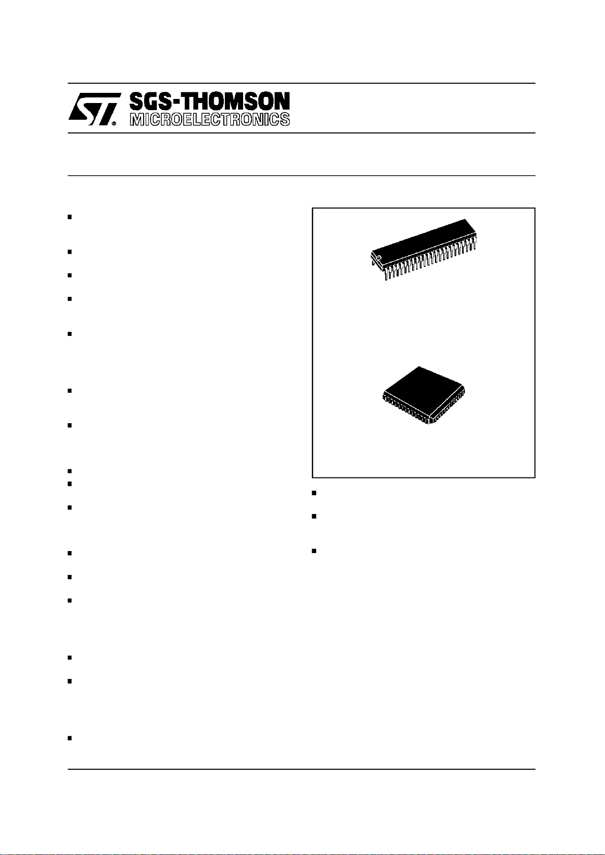
Availablein 52 pin PLCC, 84 pin PLCC(foruse
with externalROM), or 48 pin DIP packages.
SECTION 2- INTRODUCTION
The SGS - Thomson MK502H5 Link Level Controller is a VLSI semiconductor device which provides complete link level data communications
control conforming to the 1984 and 1988 CCITT
versions of X.25. The MK50H25 will perform
frame formating including: frame delimiting with
flags, transparency (so-called ”bit-stuffing”), error
recovery by retransmission, sequence number
control, S (supervisory) and U (unnumbered)
frame control, plus FCS (CRC) generation and
detection. The MK50H25 also supports X.75 and
X.32 (with its XID frame support), as well as single channel ISDN LAPD (with its support of UI
frames andextended addressingcapabilities).
July 1994
DIP48
PLCC 52
1/64
For added flexibility a transparent mode provides
an HDLC transport mechanism without link layer
support. This flexible transparent mode may be
easily entered and exited without affecting the
X.25 link status or the link statevariables kept by
the MK50H25. In this mode no protocolprocessing is done and it is up to the user to takecare of
the upper level software. Single or extended Address field filtering and Control field handling are
optionallysupported withinthe transparentmode.
One of the outstanding features of the MK50H25
is its buffer management which includes on-chip
dual channel DMA. This feature allows users to
receive and transmit multiple data frames at a
time. (A conventionalserial communications control chip plus a separate DMA chip would handle
data for only a single block at a time.) The
MK50H25 will move multiple blocks of receive
and transmit data directly into and out of memory
through the Host’s bus. A possible system configurationfor the MK50H25 is shown in figure1.
The MK50H25 may be used with any of several
popular 16 and 8 bit microprocessors, such as
68020, 68000, 6800, Z8000, Z80, 8086, 8088,
80186, 80286,80386SX, etc.
The MK50H25 may be operated in either full or
half duplex mode. In half duplex mode, the RTS
and CTSmodem control pinsare provided. In full
duplex mode, these pins become user programmable I/O pins. All signal pins on the MK50H25
are TTL compatible. This has the advantage of
making theMK50H25 independentof the physical
interface. As shown in figure 1, line drivers and
receivers are used for electrical connectionto the
physicallayer.
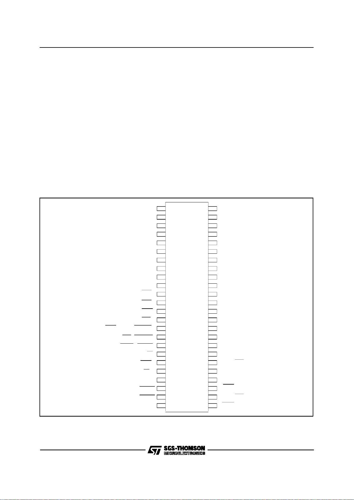
DESCRIPTION (Continued)
VSS-GND
DAL07
DAL06
DAL05
DAL04
DAL03
DAL02
DAL01
DAL00
READ
INTR
DALI
DALO
DAS
BMO, BYTE,BUSREL
BMI, BUSAKO
HOLD, BUSRQ
ALE, AS
CS
ADR
READY
RESET
VSS-GND
24
HLDA
1
2
3
4
5
6
7
8
9
10
11
12
13
14
48
47
46
45
44
43
42
41
40
39
38
37
36
23
22
21
20
19
18
17
16
15
35
34
33
32
31
30
29
28
27
26
25
TCLK
A18
A19
A20
A21
A22
A23
RD
DSR, CTS
TD
SYSCLK
RCLK
DTR, RTS
VCC (+5V)
DAL08
DAL09
DAL10
DAL11
DAL12
DAL13
DAL14
DAL15
A16
A17
M
K
5
0
H
2
5
DIP48 PIN CONNECTION (Topview)
MK50H25
2/64

VSS
DAL07
DAL06
DAL05
DAL04
DAL03
DAL02
DAL01
DAL00
READ
INTR
DALI
DALO
DAS
8
7 1 52 47
46
34
33
21
20
BMO/BYTE/BUSREL
No Connect
BM1/BUSAKO
HOLD/BUSRQ
ALE/AS
HLDA
CS
ADR
READY
RESET
VSS(GND)
TCLK
No Connect
DTR/RTS
RCLK
SYSCLK
TD
DSR/CTS
RD
A23
No Connect
A22
A21
A20
A19
A18
A17
A16
DAL15
DAL13
DAL14
VCC
DAL08
DAL09
DAL10
DAL11
DAL12
No Connect
MK50H25Q
PLCC52PIN CONNECTION (Top view)
MK50H25
3/64

SIGNAL NAME PIN(S) TYPE DESCRIPTION
DAL<15:00> 2-9
40-47
[2-10
44-51]
IO/3S The timemultiplexed Data/Address bus. During the address portion of a
memory transfer, DAL<15:00> contains the lower16 bits of the memory
address.
During the data portion of a memory transfer, DAL<15:00> contains the read
orwrite data, depending on the type of transfer.
READ 10
[11]
IO/3S READ indicatesthe type of operation that thebus controller is performing
during a bus transaction. READ is driven by the MK50H25 onlywhile it is the
BUS MASTER. READ is valid duringthe entirebus transaction and is
tristatedat all other times.
MK50H25 as a Bus Slave :
READ = HIGH - Data is placed on the DAL lines by the chip.
READ = LOW - Data is taken offthe DAL lines by the chip.
MK50H25 as a Bus Master :
READ = HIGH - Data is taken off the DAL lines by the chip.
READ = LOW - Data is placedon the DAL lines by the chip.
INTR 11
[12]
O/OD INTERRUPT is an attention interruptline that indicatesthat one or more of
thefollowing CSR0 status flagsis set: MISS, MERR, RINT, TINT or PINT.
INTERRUPT is enabled by CSR0<09>, INEA=1.
DALI 12
[13]
O/3S DAL IN is anexternal bus transceiver control line. DALI isdriven by the
MK50H25 onlywhile it isthe BUS MASTER. DALIis asserted by the
MK50H25 when it reads from the DAL linesduring the dataportion of a
READ transfer. DALIis not asserted during a WRITE transfer.
DALO 13
[14]
O/3S DAL OUT is an externalbus transceivercontrol line. DALO is driven by the
MK50H25 onlywhile it isthe BUS MASTER. DALOis asserted bythe
MK50H25 when it drives the DAL linesduring the address portionof a READ
transferor for the durationof a WRITE transfer.
DAS 14
[15]
IO/3S DATA STROBE defines thedata portion of a bus transaction. By definition,
datais stable and valid at thelow to high transition of DAS. This signalis
drivenby the MK50H25 whileit is the BUS MASTER. During theBUS
SLAVEoperation, this pin is used as an input. At allother times the signalis
tristated.
BMO
BYTE
BUSREL
15
[16]
IO/3S I/O pins 15 and 16 are programmable throughCSR4. If bit 06 ofCSR4 is set
to a one, pin 15becomes input BUSREL and is used by the host to signal
theMK50H25 to terminate a DMAburst afterthe current bus transfer has
completed. If bit 06 isclear then pin15 is an output and behaves as
described below for pin 16.
BM1
BUSAKO
16
[18]
O/3S Pins15 and 16 are programmable throughbit 00 ofCSR4 (BCON).
If CSR4<00> BCON = 0,
I/O PIN 15= BMO (O/3S)
I/O PIN 16 = BM1(O/3S)
BYTE MASK<1:0> Indicates the byte(s) on the DAL to be reador written
during this bus transaction. MK50H25 drives these lines onlyas a Bus
Master. MK50H25 ignoresthe BM lineswhen it is a Bus Slave.
Byte selection is done as outlined in the following table.
BM1 BM0 TYPE OF TRANSFER
LOW LOW ENTIRE WORD
LOW HIGH UPPER BYTE
(DAL<15:08>)
HIGH LOW LOWER BYTE
(DAL<07:00>)
HIGH HIGH NONE
TAble 1: PIN DESCRIPTION
LEGEND:
I Inputonly O Outputonly
IO Input / Output 3S 3-State
OD Open Drain(no internalpull-up)
Note: Pin out for 52 pin PLCCis shownin brackets.
MK50H25
4/64
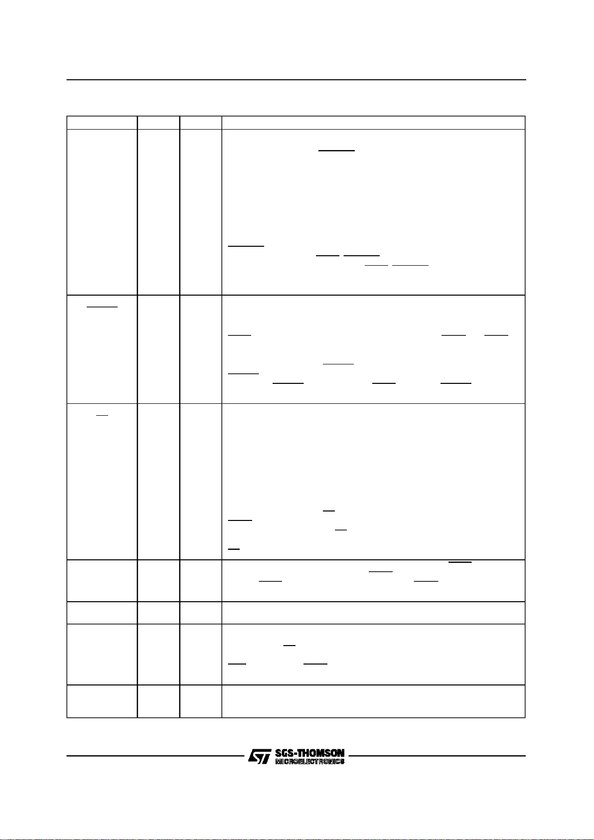
Table 1: PIN DESCRIPTION (continued)
SIGNAL NAME PIN(S) TYPE DESCRIPTION
If CSR4<00> BCON = 1,
I/O PIN 15 = BYTE (O/3S)
I/O PIN 16 = BUSAKO(O)
Byte selection is done using the BYTE lineand DAL<00> latched during the
addressportion of the bus transaction. MK50H25 drives BYTE only as a Bus
Master andignores it when a Bus Slave. Byte selectionis done as outlined
in the following table.
BYTE DAL<00> TYPE OF TRANSFER
LOW LOW ENTIRE WORD
LOW HIGH ILLEGAL CONDITION
HIGH LOW LOWER BYTE
HIGH HIGH UPPER BYTE
BUSAKOis a bus request daisy chainoutput. If MK50H25 isnot requesting
thebus and it receivesHLDA, BUSAKOwill be driven low. If MK50H25 is
requesting the bus when it receives HLDA, BUSAKOwill remain high
Note: Alltransfers areentire word unless the MK50H25 is configuredfor 8 bit
operation.
HOLD
BUSRQ
17
[19]
IO/OD Pin 17 is configured through bit 0 of CSR4.
If CSR4<00> BCON = 0,
I/O PIN 17= HOLD
HOLD request is asserted by MK50H25 when it requires a DMA cycle, if
HLDA is inactive, regardless of the previous state of the HOLDpin. HOLDis
heldlow for the entireensuing bus transaction.
If CSR4<00> BCON = 1,
I/O PIN 17 =BUSRQ
BUSRQ is asserted by MK50H25 whenit requires a DMA cycle if the prior
state of the BUSRQ pin was high andHLDA is inactive. BUSRQ is held low
for the entire ensuing bus transaction.
ALE
AS
18
[20]
O/3S The active level of ADDRESS STROBE is programmable through CSR4.
The addressportion of a bus transfer occurswhile this signal is at its
asserted level. This signal is driven by MK50H25 while it is the BUS
MASTER. At allother times, the signalis tristated.
If CSR4<01> ACON = 0,
I/O PIN 18 =ALE
ADDRESS LATCH ENABLE is used to demultiplex the DAL linesand define
theaddress portion of the transfer. As ALE, the signal transitions from high
to low during the address portion of thetransfer and remains low duringthe
dataportion.
If CSR4<01> ACON = 1,
I/O PIN 18 =AS
As AS, thesignal pulses low during the address portion of the bus transfer.
The lowto high transition of AScan be used by a slave device to strobe the
addressinto a register.
AS is effectively the inversionof ALE.
HLDA 19
[21]
I HOLD ACKNOWLEDGE is the response to HOLD. When HLDA is low in
response to MK50H25’s assertion of HOLD, the MK50H25 is the Bus
Master. HLDA should be deasserted ONLY after HOLD has been released
by theMK50H25.
CS 20
[22]
I CHIP SELECT indicates,when low, that the MK50H25 is the slave device
for the data transfer. CS must be validthroughout the entiretransaction.
ADR 21
[23]
I ADDRESS selects the Register Address Portor the Register Data Port. It
must be valid throughout the data portion of the transfer and is onlyused by
thechip when CS is low.
ADR PORT
LOW REGISTER DATA PORT
HIGH REGISTER ADDRESS PORT
READY 22
[24]
IO/OD When the MK50H25 is a Bus Master, READY is an asynchronous
acknowledgement from the bus memory thatmemory will accept data in a
WRITE cycle or that memory hasput data on the DAL linesin a READ cycle.
MK50H25
5/64
Table1: PINDESCRIPTION (continued)
SIGNAL NAME PIN(S) TYPE DESCRIPTION
As a Bus Slave, the MK50H25 asserts READY whenit has put data on the
DAL lines during a READ cycle or is about to take data from theDAL lines
during aWRITE cycle. READY is a response to DAS and it will be released
after DAS or CS is negated.
RESET 23
[25]
I RESET is the Bus signalthat will causeMK50H25 to cease operation, clear
its internal logic and enter an idlestate with thePower Off bit ofCSR0 set.
TCLK 25
[28]
I TRANSMIT CLOCK. A1x clock inputfor transmitter timing. TD changes on
the fallingedge of TCLK. The frequency of TCLK may not be greater than
the frequency of SYSCL
DTR
RTS
26
[29]
IO DATA TERMINAL READY, REQUEST TO SEND. Modem controlpin. Pin
26 is configurable throughCSR5. This pin can be programmed to behave as
output RTS or as programmable IO pin DTR. Ifconfigured as RTS, the
MK50H25 will assert this pin if it has data to send and throughout the
transmission of a signal unit.
RCLK 27
[30]
I RECEIVE CLOCK. A 1xclock input for receiver timing. RD issampled on
the risingedge of RCLK. The frequency of RCLK may not be greater than
the frequency of SYSCLK.
SYSCLK 28
[31]
I SYSTEM CLOCK. System clock used for internal timing of the MK50H25.
SYSCLK should be a square wave, of frequency up to 33 MHz.
TD 29
[32]
O TRANSMIT DATA. Transmit serial data output.
DSR
CTS
30
[33]
IO DATA SET READY, CLEAR TO SEND.Modem Control Pin.Pin 30 is
configurablethrough CSR5. This pin can be programmed to behave as input
CTS or as programmable IO pin DSR. If configured as CTS,the MK50H25
will transmitall ones whileCTS is high.
RD 31
[34]
I RECEIVE DATA. Received serial data input.
A<23:16> 32-39
[37-43]
o/3s Address bits <23:16>used in conjunction with DAL<15:00> toproduce a 24
bit address. MK50H25 drives these lines only as a Bus Master. A23-A20
may be driven continuously as describedin the CSR4<7>BAE bit.
VSS-GND 1,24
[1,26]
Ground Pins
VCC 48
[52]
Power Supply Pin
+5.0 VDC + 5%
SECTION3
OPERATIONALDESCRIPTION
The SGS-Thomson MK50H25 Multi-Logical Link
CommunicationsControllerdevice isa VLSIproduct intended for high performancedata communication applications requiring X.25 link level control. The MK50H25 will perform all frame
formatting, such as: frame delimiting with flags,
FCS (CRC) generation and detection, and zero
bit insertion and deletion for transparency. The
MK50H25 also handles all supervisory (S) and
unnumbered (U) frames (see Tables A & B). The
MK50H25 also includes a buffer management
mechanismthat allowsthe user totransmit and/or
receive multiple frames for each active channel
or DLCI. Contained in the buffer management is
an on-chip dual channel DMA:one channel for receiveand one channelfor transmit.
The MK50H25 can be used with any popular 16
or 8 bit microprocessor. A possible system configuration for the MK50H25 is shown in Figure 1.
This document assumesthat the processorhas a
byte addressablememoryorganization.
The MK50H25 will move multiple blocks of receive and transmit data directly in and out of
memory throughthe Host’sbus.
The MK50H25 may be operated in full or half duplex mode. In half duplex mode the RTS and
CTS modem control pins are provided. In full duplex mode, these pins become user programmable I/O pins.
All signalpins on the MK50H25 are TTL compatible. This has the advantage of making the
MK50H25 independent of the physical interface.
As shown in Fig. 1, line drivers and receiversare
used for electrical connection to the physical
layer.
MK50H25
6/64
HOST PROCESSOR
(68000, 80186, Z8000, ETC)
16-BIT DATA BUS INCLUDING
24-BIT ADDRESS AND BUS CONTROL
MEMORY
(MULTIPLE
DATA BLOCKS)
MK50H25
RD
TD
LINE DRIVERS
AND RECEIVERS
(SUCH AS RS-449, RS-232C, V.35)
DATA COMM. CONNECTOR
ELECTRICAL I/O
(SUCH AS RS-232C, RS-423, RS-422)
TCLK
RCLK
DSR, CTS
DTR, RTS
Figure1: Possible System Configurationfor thr MK50H25
MK50H25
7/64

DALI
DALO
HLDA
HOLD
ALE, AS
BM0
BM1
DAS
READ
INTR
ADR
READY
DTR, RTS
DSR, CTS
CS
FIRMWARE
ROM
MICRO
CONTROLLER
TIMERS
DMA
CONTROLLER
CONTROL / STATUS
REGISTERS 0 - 5
SYSCLK
INTERNAL BUS
RECEIVER
FIFO
TRANSMITTER
FIFO
RECEIVER TRANSMITTER
LOOPBACK
TEST
RD
RCLK
TCLK
TD
VSS - GND
RESET
VCC
DAL<15:00>
A <23:16>
Figure2: MK50H25Simplified BlockDiagram
MK50H25
8/64

3.1 FunctionalBlocks
Refer tothe blockdiagram in Figure2.
The MK50H25 is primarily initialized and control-
led through six 16-bit Control and Status Registers (CSR0 thru CSR5). The CSR’s are accessed
through two bus addressable ports, the Register
Address Port (RAP), and the Register Data Port
(RDP). The MK50H25 may also generate an interrupt(s) to the Host. These interrupts are enabledand disabled throughCSR0.
The on-chip microcontroller is used to control the
movement of parallel receive and transmit data,
and to handle the Addressfield filtering.
3.1.1 Microcontroller
Themicrocontroller controlsall of the otherblocks
of the MK50H25. The microcontroller performs
frame processing and protocol processing. All
primitive processing and generation is also done
here. The microcode ROM contains the control
programof the microcontroller.
3.1.2 Receiver
Serial receive data comes into the Receiver (Figure 2). The Receiver is responsiblefor:
1.Leading and trailingflag detection.
2.Deletion of zeroesinserted for transparency.
3.Detection of idle and abort sequences.
4.Detection of good and bad FCS (CRC).
5. MonitoringReceiverFIFO status.
6.Detection of ReceiverOver-Run.
7. Oddbyte detection.
NOTE: If framesare receivedthat have an odd
numberof bytes then thelast byteof the
frame is said to be anodd byte.
8.Detection of non-octet aligned frames.Such
framesare treated as invalid (CCITT X.25 sec
2.3.5.3)
3.1.3 Transmitter
The Transmitteris responsiblefor:
1. Serializationof outgoingdata.
2. Generatingand appendingthe FCS(CRC).
3. Framing outgoingframe with flags.
4. Zerobit insertion fortransparency.
5. TransmitterUnder-Run detection.
6. Transmissionof odd byte.
7.RTS/CTScontrol.
3.1.4 Frame Check Sequence orCyclic
Redundancy Check
The FCS (CRC) on the transmitter or receiver
may be either 16 bit or 32 bit, and is user selectable. For full duplex operation, both the receiver
and transmitter have individual FCS computation
circuits. The characteristics ofthe FCS are:
TransmittedPolarity: Inverted
TransmittedOrder: High OrderBit First
Pre-setValue: All 1’s
Polynomial16 bit:
X
16+X12+X5
+1
Remainder16 bit (if received correctly):
Highorder bit-->0001 11010000 1111
Polynomial32 bit:
X
32+X26+X23+X22+X16+X12+X11+X10
+
X
8+X7+X5+X4+X2
+X+1
Remainder32 bit (if received correctly):
high order bit-->1100 0111 00000100
1101 11010111 1011
3.1.5 Receive FIFO
The Receive FIFO buffers the data received by
the receiver. This performs two major functions.
First, it resynchronizes the data from the receive
clock to the system clock. Second, it allows the
microcontroller time to finish whatever it may be
doing beforeit has to processthe receiveddata.
The receiveFIFO holds the data from the receiver
without interrupting the microcontroller for service
until it contains enough data to reach the watermark level, or an end of frame is received. This
watermark level can be programmed in CSR4
(FWM) to occur when the FIFO contains at least
18 or more bytes; 34 or more bytes; or 50 or
more bytes. This programmability, along withthe
programmableburst length of the DMAcontroller,
enables the user to definehow often and for how
long the MK50H25 must use the host bus. For
more information,see CSR4.
For example, if the watermark level is set at 34
bytes and the burst length is limited to 8 word
transfers at a time, the MK50H25 will request
control of the host bus as soon as 34 bytes are
received and again after every 16 subsequent
bytes.
3.1.6 Transmit FIFO
The Transmit FIFO buffers the data to be transmitted by the MK50H25. This also performs two
major functions. First, it resynchronizesthe data
from the systemclock to the transmitclock. Second, it allows the microcontroller and DMA controller to burst read data from the host’s memory
buffers; making both the MK50H25 and the host
bus more efficient.
The transmit FIFO hasa watermarkscheme similar to the one described for the receive FIFO
above, and uses the sameFWM value selections
in CSR4 for the watermark. Once filled to within
MK50H25
9/64

FWM of being full (by DMA from TX buffer in
shared memory), the transmit FIFO will not interrupt the microcontroller until it emptiesenough to
fall below the watermarklevel.
The transmit FIFO also has a selectableTransmit
Hold-Off watermark mechanism to determine
when data transmission will begin once data has
been put in the transmit FIFO. The Transmit
Hold-Off watermark is enabled by setting bit 10
(XHOLD) in CSR4. The selection of FWM (FIFO
WaterMark) also in CSR4 determines corresponding appropriate values of TransmitHold-Off
so that the device cannot be inadvertently programmed to have conflicting watermarks. For
FWM settings of 9, 17, and 25 words, the Transmit Hold-Off watermarks are 19, 11, and 3 words
respectively.
For example, if FWM is set at 9 words and the
Transmit Hold-Off watermark is enabled, the
MK50H25 will not begin transmitting until more
than 19 words have been placed in the Transmit
FIFO or an end-of-frame has been transmitted.
This greatly reduces the chances of Transmitter
Underrunthat could be possible at highdata rates
(ie: TCLK > 0.15 x SYSCLK) if Transmit Hold-Off
is not selected (causing transmission to begin as
soonas 1byte is transferredto the TX FIFO).
3.1.7 DMA Controller
TheMK50H25 has an on-chip DMAControllercircuit. This allows it to access memory without requiring host software intervention. Wheneverthe
MK50H25 requires access to the host memory it
will negotiate for mastership of the bus. Upon
gainingcontrol of thebus the MK50H25 willbegin
transferring data to or from memory. The
MK50H25 will perform memory transfers until
either it has nothing more to transfer, it has
reached its DMA burst limit (user programmable),
or the BUSREL pin is driven low. In any case, it
will complete all bus transfers before releasing
bus mastership back to the host. If during a
memory transfer, the memory does not respond
within 256 SCLK cycles, the MK50H25 will release ownership of the bus immediately and the
MERR bit will be set in CSR0. The DMA burst
limit can be programmed by the user through
CSR4. In 16 bit mode the limit can be set to 1
word, 8 words, or unlimited word transfers. In 8
bit mode,it can be set to 2 bytes, 16 bytes, or unlimited byte transfers. For high speed data lines
(i.e. > 1 Mbps)a burst limit of 8 words or 16 bytes
issuggested to allow maximumthroughput.
The byte ordering of the DMA transfers can be
programmedto account for differencesin processor architectures or hostprogramming languages.
Byte ordering can be programmed separately for
data and control information. Data information is
defined as all contents of data buffers; control information is defined as anything else in the
shared memoryspace (i.e. initialization block,descriptors, etc). For more information see section
4.1.2.5 on control statusregister 4.
3.1.8 Bus Slave Circuitry
The MK50H25 contains a bank of internal control/status registers (CSR0-5) which can be accessed by the hostas a peripheral. The host can
read or write to these registers like any other bus
slave. The contents of these registers are listed
in Section4 and bus signal timing is described in
Figures 9and 10.
3.2 Buffer ManagementOverview
Refer to Fig.3.
3.2.1 Initalization Block
Chip initialization information is located in a block
of memory called the Initialization Block. The Initialization Block consists of 25 contiguous words
of memory starting on a word boundary. This
memory is assembled by the HOST, and is accessed by the MK50H25during initialization. The
InitializationBlock iscomprised of:
A. Modeof Operation.
B. FrameAddress Values.
C. N1 Counter (Max FrameLength) Value.
D. Timer Preset Values
E. Locationand size ofReceive and TransmitDe-
scriptor Rings.
F. Locationand size ofXID/TEST Buffers.
G. Location ofStatus Buffer.
H. ErrorCounters.
3.2.2 The Circular Queue
The basic organization of the buffer management
is a circular queue of tasks in memory called descriptor rings. There are separate rings to describe the transmit and receive operations. Up to
128 buffers may be queued-up on a descriptor
ring awaiting execution by the MK50H25. The
descriptor ring has a descriptor assignedto each
buffer. Each descriptor holds a pointer for the
starting address of the buffer, and holds a value
for the lengthof the bufferin bytes.
Each descriptor also contains two control bits
called OWNA and OWNB, which denote whether
the MK50H25, the HOST, or the I/O ACCELERATION PROCESSOR( if present ) ”owns” the buffer. For transmit, when the MK50H25 owns the
buffer, the MK50H25 is allowed and commanded
to transmit the buffer. When the MK50H25 does
not own the buffer, it will not transmit that buffer.
For receive, when the MK50H25owns a buffer, it
may place received data into that buffer. Conversely, when the MK50H25 does not own a receive buffer, it will not place received data into
that buffer.
The MK50H25 buffer management mechanism
will handle frames which are longer than the
length of an individual buffer. This is done by a
chaining method which utilizes multiple buffers.
The MK50H25 tests the next descriptor in the de-
MK50H25
10/64
scriptor ring in a ”look ahead” manner. If the
frame is too long for one buffer, the next buffer
will be used after filling the first buffer; that is,
”chained”. The MK50H25 will then ”look ahead”
to the next buffer, and chain that buffer if necessary, and so on.The operational parameters for
the buffer managementare defined by the user in
the initialization block. The parameters defined
include the basic mode of operation, the number
of entries for the transmitter and receiver descriptor rings, frame Address field, etc. The starting
address for the Initialization block, IADR, is defined in the CSR2 and CSR3 registers inside the
MK50H25.
3.2.3 FrameFormat
The frame format supported by the MK50H25 is
shown below. Each frame may consistof a programmable number of leading flag patterns
(01111110), an address field, a control field, an
informationfield, an FCS (CRC) ofeither 16 or 32
bits, and a trailing flag pattern. The number of
leading flags transmitted is programmable
through the Mode Register in the Initialization
Block. Received frames may have as few as one
flagbetween adjacentframes
TRANSMITTED FIRST
3.2.4 TheCommand/ResponseRepertoire
The command/response repertoire of the
MK50H25 is shown in Tables A and B. This set
conforms to the 1984 & 1988 CCITT X.25, plus
supportof XID, Test,and UI frames conformingto
ISDN LAPD. The MK50H25 will process the Information, Supervisory, and Unnumbered frames
shown in Tables A and B, and will handle the A
and C fieldsfor all I and UIframes.
The symbols and definitions for the frame types
are:
Name Definition
I Information frame
UI Unnumbered Information frame
RR ReceiverReady
RNR Receiver Not Ready
REJ Reject
FRMR Frame Reject
UA Unnumbered Acknowledge
SABM Set Asynchronous Balance Mode
DISC Disconnect
DM Disconnect Mode
TEST Link Test Frame
XID Exchange Identification
AC
INFO
F
8/16 8/16
8*n
8
F FCS
8
16/32
MK50H25
11/64

Table A - MK50H25Command/Response Repertoire
Modulo 8 Operation
FORMAT COMMAND RESPONSE ENCODING
LSB MSB
12345678
InformationTransfer I I 0 ← N(S)
→ P ← N(R) →
Supervisory RR RR 1 0 0 0 P/F ← N(R) →
RNR RNR 1 0 1 0 P/F ← N(R) →
REJ REJ 1 0 0 1 P/F ← N(R) →
Unnumbered
*
UI
*
UI 1100P/F000
SABM 1 1 1 1 P 1 0 0
DM 1111F000
DISC 1 1 0 0 P 0 1 0
UA 1100F110
FRMR 1 1 1 0 F 0 0 1
*
XID
*
XID 1 1 1 1 P/F 1 0 1
TEST TEST 1 1 0 0 P/F 1 1 1
Table B - MK50H25Command/Response Repertoire
Modulo128 Operation
FORMAT COMMAND RESPONSE ENCODING
LSB MSB
1 2 3 4 5 6 7 8 9 10-16
Information
Transfer
I I 0 N(S) P N(R)
Supervisory RR RR 1 0 0 0 0 0 0 0 P/F N(R)
RNR RNR 1 0 1 0 0 0 0 0 P/F N(R)
REJ REJ 1 0 0 1 0 0 0 0 P/F N(R)
Unnumbered SABME 1 1 1 1 P 1 1 0 N/A
All Others AllOthers
Same Repertoire and Encoding as forModulo 8
Notes:
1. N(S) = Transmitter Send Sequence Number
2. N(R) =Transmitter Receive Sequence Number
3. P/F = Poll bit when issued as acommand. Final bit when issued as a response.
4. N/A = Not Applicable. All Unnumbered frames have only an 8 bitControl Field for Modulo 128 orModulo 8 operation.
*XID and UI frames can be enabled individually by setting the appropriate bits in CSR2.
MK50H25
12/64

RECEIVER DESCRIPTOR RINGS
DESCRIPTOR 0
BUFFER STATUS
BUFFER ADDRESS
BUFFER SIZE
BUFFER MSG COUNT
DESCRIPTOR 1
DESCRIPTOR M
TRANSMIT DESCRIPTOR RINGS
DESCRIPTOR 0
BUFFER STATUS
BUFFER ADDRESS
BUFFER SIZE
BUFFER MSGCOUNT
DESCRIPTOR 1
DESCRIPTOR N
BUFFER
N
BUFFER
1
BUFFER
0
TRANSMIT BUFFER
BUFFER
M
BUFFER
1
BUFFER
0
RECEIVE BUFFER
CSR 2, CSR3
POINTER TO
INITIALIZATI ONBLOCK
INITIALIZATI ONBLOCK
MODE
TIMER VALUES
RX DESCRIPTOR
TX DESCRIPTOR
POINTER
POINTER
FRAME ADDRESS
FIELDS
STATUS
BUFFER ADDRESS
STATUS BUFFER
ERROR COUNTERS
XID/TEST TRANSMIT
DESCRIPTOR POINTER
XID/TEST RECEIVE
DESCRIPTOR POINTER
RECEIVE BUFFER
TRANSMIT BUFFER
XID/TEST
XID/TEST
Figure3: MK50H25Memory ManagementStructure
MK50H25
13/64
SECTION4
PROGRAMMING SPECIFICATION
This section defines the Control and Status Registers and the memory data structuresrequired to
programthe MK50H25.
4.1 Control andStatus Registers
There are six Control and Status Registers
(CSR’s) resident within the MK50H25. The
CSR’s are accessed through two bus addressable ports, an address port (RAP), and a data
port (RDP), thus requiring only two locations in
the system memory orI/O map.
4.1.1 Accessin gthe Control &StatusRegiste rs
The CSR’s are read (or written) in a two step operation. Theaddress of theCSR is written into the
address port (RAP) during a bus slave transaction. During a subsequentbus slave transaction,
the data being read from (or written into) the data
port (RDP) is read from (or written into) the CSR
selected in the RAP. Once written, the addressin
RAP remains unchanged until rewritten or upon a
bus reset. A control I/O pin (ADR) is provided to
distinguishthe addressport from the data port.
ADR Port
L RegisterData Port(RDP)
H Register AddressPort (RAP)
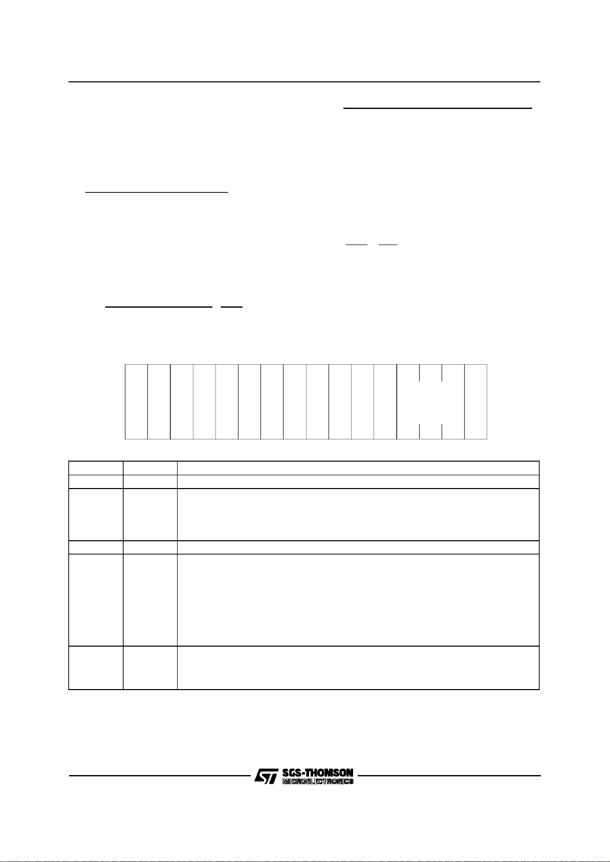
4.1.1.1 Register Address Port (RAP)
00000000
B
M
8
000
CSR
<2:0>
15141
3
0
7
0
8
1
0
1
1
1
2
0
1
0
2
0
3
0
4
0
5
0
0
0
9
0
6
H
B
Y
E
T
BIT NAME DESCRIPTION
15:08 RESERVED Must be written as zeroes
07 BM8 When set, places chip into 8 bitmode. CSR’s, Init Block, and data transfersare all 8bit
transfers; this providescompatibility with 8 bitmicroprocessors. When clear, alltransfers
are 16 bit transfers. This bit must be set to the same value each time it is written,
changing this bit during normal operation will achieve unexpected results. BM8 is
READ/WRITE and cleared on Bus RESET.
06:04 RESERVED Must be written as zeroes
03:01 CS3<2:0> CSR address selectbits. READ/WRITE. Selects the CSR to be accessed through the
RDP. RAP is cleared by Bus RESET.
CSR<2:0> CSR
0 CSR0
1 CSR1
2 CSR2
3 CSR3
4 CSR4
5 CSR5
00 HBYTE Determines which byte is addressed for 8 bit mode. If set, the high byteof the register
referred to byCSR<2:0> is addressed,otherwise the low byte is addressed. This bit is
only meaningful in8 bit mode and must be writtenas zero if BM8=0. HBYTE is
READ/WRITE and cleared on bus reset.
MK50H25
14/64

CSR DATA
1
5
1
0
1
4
0
9
121
1
0
8
0
3
0
7
0
2
06050
4
010
0
1
3
4.1.1.2 Register Data Port (RDP)
BIT NAME DESCRIPTION
15:00 CSR DATA Writing data tothe RDP loadsdata into the CSR selectedby RAP. Reading the data from
RDP reads the data from the CSR selected inRAP.
MK50H25
15/64

4.1.2 Control and Status Register Definition
4.1.2.1 Controland Status Register 0 (CSR0)
RAP<3:1> =0
BIT NAME DESCRIPTION
15 TDMD TRANSMITDEMAND, when set, causes the MK50H25 access the
Transmit Descriptor Ring without waiting for the Transmit poll time interval to lapse. TDMD need not be set to transmit a frame, it merely
hastens the MK50H25’s response to a Transmit Descriptor Ring entry
insertion by the host. TDMD is written with ONE ONLY and cleared by
the MK50H25 microcode after it is used. It may read as a ”1” for a
short time after it is written because the microcode may have been
busy when TDMDwas set. Itis also cleared byBus RESET. Writing a
”0” in this bithas no effect.
14 STOP STOP,when set, indicatesthat MK50H25 is operatingin theStopped
phase of operation. All externalactivity is disabled and internallogic is
reset. MK50H25 remainsinactive except for primitive processing until
a START primitive is issued. STOP IS READ ONLY and set by Bus
RESET ora STOP primitive. Writing to thisbit has no effect.
13 DTX DisableTransmitter ring prevents the MK50H25from furtheraccess to
the Transmitter Descriptor Ring. No transmissions are attempted after
finishing transmission of any frame in transmission at the time of DTX
being set. TXON acknowledgeschanges to DTX, see below. DTX is
READ/WRITE.
12 DRX Disable theReceiver prevents the MK50H25 fromfurther access tothe
Receiver Descriptor Ring. No received frames are accepted after finishing receptionof any frame in receptionat the time of DRX being set.
If DRX is set while a data link is established, the MK50H25 will go into
the Local Busy state and will send an RNR response frame to the remote station. Upon clearing DRX the MK50H25 will send a RR response frame. RXON acknowledges changes to DRX, see description
of RXON. DRX is READ/WRITE.
11 TXON TRANSMITTER ON indicates that thetransmit ring accessis enabled.
TXON is setas the Startprimitive is issuedif theDTX bit is ”0” or afterward as DTX is cleared. TXON is clearedupon recognition of DTXbeing set, by sending a Stop primitive in CSR1, or by a Bus RESET. If
TXON is clear, the host may modify the Transmit Descriptor Ring entries regardless of the state of the OWNA bits. TXON is READ ONLY;
writing to thisbit has no effect.
10 RXON RECEIVERON indicates that the receive ring access is enabled.
RXON isset as the Startprimitive isissued if the DRX bit is ”0” or afterward as DRX is cleared. RXON is cleared upon recognition of DRX
being set, by sendinga Stop primitive in CSR1, or by a Bus RESET. If
RXON is clear, the host may modify the Receive Descriptor Ring entries regardless of the state of the OWNA bits. RXON is READ ONLY;
writing to thisbit has no effect.
15141
3
0
7
0
8
1
0
1
1
1
2
0
1
0
2
0
3
0
4
0
5
0
0
0
9
0
6
0
R
I
N
T
T
I
N
T
P
I
N
T
T
U
R
M
I
S
S
M
E
R
R
R
O
R
I
N
T
R
R
X
O
N
T
X
O
N
I
N
E
A
S
T
O
P
D
T
X
D
R
X
P
T
D
M
D
MK50H25
16/64

09 INEA INTERRUPT ENABLEallows the INTRI/O pin to be driven lowwhen
the InterruptFlag is set. If INEA = 1 and INTR = 1 the INTR I/Opin will
be low. If INEA = 0 the INTR I/O pin will be high, regardless of the
state of the Interrupt Flag. INEA is READ/WRITE set by writinga
”1” into this bit and is cleared by writing a ”0” into this bit, by Bus RESET, or by issuing a Stop primitive. INEA may not be set while in the
Stopped phase.
08 INTR INTERRUPT FLAGindicatesthat one or moreof the following interrupt
causing conditions has occurred: MISS, MERR, RINT, TINT, PINT,
TUR or ROR. If INEA = 1 and INTR = 1 the INTR I/O pin will be low.
INTR is READ ONLY,writing this bithas no effect.INTR is cleared as
the specific interrupting condition bits are cleared. INTR is also
cleared byBus RESETor byissuing a Stopprimitive.
07 MERR MEMORYERROR is set when theMK50H25is the Bus Masterand
READY has not been asserted within 256 SYSCLKs (25.6 usec @
10MHz) after assertingthe address on the DAL lines. When a Memory Error is detected, the MK50H25releases the bus, the receiver
and transmitter are turned off, and an interruptis generated if INEA =
1. MERR is READ/CLEARONLY and is set by the chipand clearedby
writing a ”1” into the bit. Writing a ”0” has no effect. It is cleared by
Bus RESETor by issuinga Stop primitive.
06 MISS MISSEDframe is set when the receiverloses a framebecause it does
not own a receive buffer indicating loss of data. When MISS is set,
RXON is cleared and an interrupt will be generated if INEA = 1. If
MISS is set while a data link is established, the MK50H25 will go into
the Local Busy state and will send an RNR response frame to the remote station. Upon clearing MISS the MK50H25 will send a RR response frame. MISS is READ/CLEAR ONLY and is set by MK50H25
and cleared by writing a ”1” into the bit. Writing a ”0” has no effect. It
is also cleared by Bus RESETor by issuinga Stop primitive.
05 ROR RECEIVEROVERRUNindicates that the Receiver FIFOwas full when
the receiver was ready to input data to the Receiver FIFO. When ROR
occurs, the receive FIFO will be flushed and the buffer(s) containing
any part of the frame already received will be re-used by the next incomming frame. Therefore, the framebeing received is lost, but is typically recoverable through the protocol used. When ROR is set, an interrupt is generated if INEA = 1. ROR is READ/CLEAR ONLY and
is set by MK50H25 and clearedby writing a ”1” into the bit. Writing a
”0” has no effect. It is also clearedby Bus RESET or by issuing a Stop
primitive.
04 TUR TRANSMITTERUNDERRUN indicates that the MK50H25 has aborted
a frame since data was late from memory. This condition is reached
when the transmitter and transmitter FIFO both become empty while
transmitting a frame. The frame in transmission at the time will be
aborted. When TUR is set, an interruptis generatedif INEA = 1. TUR
is READ/CLEARONLY and is set by MK50H25 and cleared by writing
a ”1” into the bit. Writing a ”0” has no effect. It is also cleared by Bus
RESET orby issuing a Stop primitive.
03 PINT PRIMITIVE INTERRUPT is set after the chip updates the primitive
register to issue a provider primitive. When PINT is set, an interrupt is
generated if INEA =1. PINT is READ/CLEAR ONLY and is set by
MK50H25 andcleared by writinga ”1” into the bit. Writing a ”0” has no
effect. It isalso clearedby BusRESETor by issuing a Stop primitive.
02 TINT TRANSMITTERINTERRUPT is setafter thechip updatesan entryin
the Transmit Descriptor Ring. This occurrs when a transmitted I frame
has been acknowledged by the remote station. When transmitting UI
frames, or in TransparentMode, TINTis set upon completingtransmission of the frame. When TINT is set, an interruptis generatedif INEA
= 1. TINT is READ/CLEAR ONLY and is set by the MK50H25 and
MK50H25
17/64

cleared by writing a ”1” into the bit. Writing a ”0” has no effect. It is
also clearedby Bus RESET or by issuinga Stop primitive.
01 RINT RECEIVERINTERRUPT is set afterthe MK50H25updates an entryin
the ReceiveDescriptor Ring. This occurswhen the MK50H25has successfuly received an I, UI, or FRMR frame, and any good frame in
Transparent Mode. When RINT is set, an interrupt is generated if
INEA = 1. RINT is READ/CLEAR ONLY and is set by the MK50H25
and clearedby writing a ”1” into the bit.Writing a ”0” has no effect. Itis
cleared byBus RESETor byissuing a Stopprimitive.
00 0 This bit isREAD ONLYand will alwaysread as a zero.
4.1.2.2 Controland Status Register 1 (CSR1)
RAP <3:1> = 1
BIT NAME DESCRIPTION
15 UERR USERPRIMITIVEERROR isset bythe MK50H25 when a primitive is
issued by the user which is in conflict with the current status of the
chip. UERR is READ/CLEAR ONLY and is set by MK50H25 and
cleared by writing a ”1” into the bit. Writing a ”0” in this bit has no
effect. It isalso clearedby Bus RESET.
14 UAV USERPRIMITIVEAVAILABLE is set by the user whena primitiveis
written into UPRIM. It is cleared by the MK50H25 after the primitive
has been processed. This bit is also clearedby a Bus RESET.
13 UPARM USER PARAMETERis writtenby the host inconjunction with the user
primitivesin UPRIM. ThisUser Parameter field provides information to
the MK50H25 concerning the corresponding user primitive. For connect and reset primitives this field determines what the MK50H25 will
do with frames in the transmit descriptor ring which have previously
been sent but not acknowledged. If UPARM= 0, these frames will be
resent when the new link is established. If UPARM = 1, these frames
will be discarded and their OWNA bits cleared, releasing ownership
back to the host. For other primitives UPARM = 0 unless otherwise indicated.
12:08 UPRIM USER PRIMITIVEis written by the user,in conjunctionwith setting
UAV, to controlthe MK50H25link procedures. The followingprimitives
are available:
0 Stop: Causes MK50H25to enter theStopped modeor phase. All DMA
activity ceases,the transmitter transmits all ones,and all received data
is ignored. A Stop primitive issued during transmission of a frame will
cause the frame to be aborted as the Transmitter outputs 1’s. A Stop
primitive issued with UPARM=1 will cause a software Reset of the
MK50H25(equivalent to assertingthe RESETpin).
1 Start: Instructsthe MK50H25to exit the StoppedMode and enterthe
Disconnected phase, if UPARM = 0. The descriptor Rings are reset.
The transmitter begis to output flags. If issued with UPARM = 1 the
MK50H25 will directly enter the Information Transfer phase (link connected).Validonly in StoppedMode or TransparentMode.
1
5
1
0
1
4
0
9
121
1
0
8
0
3
0
7
0
2
06050
4
010
0
1
3
UPRIM
< 3:0 >
PPRIM
< 3:0 >
U
E
R
R
U
A
V
P
A
V
P
L
O
S
T
P
P
A
R
M
1
:
0
UPARM
<1:0>
MK50H25
18/64

2 Init: Instructs the MK50H25 to readthe InitializationBlock from memory.
Valid only in the Stopped mode or phase. This should be performed
prior to theStart primitiveafter a bus resetor power-up.
3 Trans: InstructsMK50H25to enterthe TransparentMode of operation.
Data frames are transmitted and received out of the descriptor rings
with no Address and Control fields prepended to the frames. If the
PROM bit is set in the Protocol Parameters register, then no address
filtering is performed on received frames. Transparent Mode may be
exited with a Stop primitive or by a bus reset. Exiting from Transparent
Mode to the informationtransfer phase (link connected) is possible by
issuing a Start primitive withUPARM= 1, or to the Disconnectedphase
by issuingStart with UPARM = 0.
4 Status Request: Instructs the MK50H25to write thecurrent chipstatus
into the STATUS BUFFER. Valid in all states, but only after the Init
primitivehas been previouslyissued.
5 Self-Test Request:Instructsthe MK50H25 toperform the built in internal
self test. Validonly in the Stopped phase. A Self Test primitiveissued
with UPARM=3 will cause the device to identify itself by returning a
Provider primitive of 5 (or 7 for the MK50H27, etc). See section 4.4.12
for the selftest procedure.
6 Connect Request:Instructs theMK50H25 to attempt to establisha logical
link with theremote station.Valid only inDisconnectedphase .
7 Connect Response:Indicates willingness to establisha logical link with
the remote station. Valid only in Disconnected phase after receiving a
Connect Indicationprimitive.
8 Reset Request:If a logical link has been established,it instructsthe
MK50H25 to attempt toreset the current link with the remote station.In
TransparentMode or Disconnected Phase,it instructs the MK50H25to
start the T1 timer (to beused as a generalpurpose timer).
9 Reset Response: If a logical link has been established, it indicates
willingness to reset the current logical link with remote station. Valid
only after receiving Reset Indication primitive. In Transparent Mode or
DisconnectedPhase, it instructs the MK50H25 to stop the T1timer.
10 XID Request: Instructsthe MK50H25 tosend a XID frame tothe remote
station. Data in the XID/TestTransmit buffer is used for the Data Field.
Invalid in StoppedMode.
11 XID Response:Instructsthe MK50H25to send an XIDresponse frameto
the remote station. Data in the XID/TEST Transmit buffer is used for
the data field.Valid onlyafter receivingan XIDIndicationprimitive.
12 TEST Request: InstructsMK50H25 tosend a TESTcommand to the
remote station. Data in the XID/TEST Transmit buffer is used for the
data field. Invalid inStopped mode.
13 TEST Response: InstructsMK50H25to send a TESTresponse frameto
the remote station. Data in XID/TEST Transmit buffer is used for the
data field. Valid onlyafter receivingTEST Indicationprimitive.
14 DisconnectRequest:Instructs the MK50H25to disconnectthe current
logical linkand enter the NormalDisconnected phase. If the linkis currently disconnected, issuing Disconnect Request with UPARM=0 will
cause a DM/F=0 frameto be sent; issuingit with UPARM=1will cause
a DISC/P=0 frame to be sent.
07 PLOST PROVIDERPRIMITIVE LOST is set by the MK50H25when a provider
primitive cannotbe issued because thePAV bit is still set from the previous provider primitive. PLOST is cleared when PAV is cleared or by
a Bus RESET. Writing to thisbit has no effect.
06 PAV PROVIDERPRIMITIVEAVAILABLEis set by theMK50H25 whena new
provider primitive has been placed in PPRIM. PAV is READ/CLEAR
MK50H25
19/64

ONLY and is setby the chip and clearedby writing a ”1” to the bit orby
Bus RESET. Under normaloperation thehost should clear thePAV bit
after PPRIM is read.
05:04 PPARM PROVIDERPARAMETERprovides additionalinformationabout the
reason for the receipt of certain primitives. The following table shows
the parametersfor the applicableproviderprimitives. This field is undefined for otherprovider primitives.
PPRIM
PPARM
Disconnect
Indication
Disconnect
Confirmation
Reset
Indication
Error
Indication
Remote Busy
Indication
0 Remotely
Initiated
UA or DMF=1
Received
Remotely
Initiated
Unsolicited
DM/F=0 Rcvd
RemoteBusy
RNRReceived
1 SABM Timeout DISC Timeout Timer
Recovery
Timeout
RemoteUnBusyRR or
REJRcvd.
2 FRMRSent the
DISC or DM
Rcvd.
FRMR Sent
then SABM/E
Received
FRMR
Received
3 T3Timeout T3 Timeout Unsolicited Ua
or F bit
Received
03:00 PPRIM PROVIDERPRIMITIVE iswritten by theMK50H25, in conjunctionwith
with setting the PAV bit, to inform the user of link control conditions.
Valid ProviderPrimitivesare as follows:
2 Init Confirmation:IndicatesMK50H25 Init Block readinghas completed.
3 Watchdog Timer Expiry Indication: Indicates expirationof TCLKor RCLK
watchdog timeras determined by the value ofPPARM. (PPARM=1indi-
cates TCLK, PPARM=2 indicates RCLK If PLOST is set it indicates
both RCLKand TCLK watchdogtimer expiry). Issuedonly if enabled.
4 Error Indication:Indicatesan Error conditionhas occurredduring the
Information Transfer phase that requires instruction by the Host for re-
covery. See the PPARM table for specificerror conditions. Appropriate
Host responsesare ConnectResponse or Disconnect Request.
5 Remote BusyIndication: Indicateschange in theRemote Busystatus of
the MK50H25. SeePPARM table for specific conditions. This primitive
is only generatedif RBSY(bit 11 of IADR+16)is set= 1.
6 Connect Indication:Indicatesattempt by the Primarystation to establish
a logical link (SABM received). Appropriate user responses are Con-
nect Responseor DisconnectRequest.
7 Connect Confirmation: Indicates sucessof a previousConnect Request
by the user. A logicallink is nowestablished.
8 Reset Indication:If a logicallink has beenestablished,it indicates an
attempt by the Primary station to reset the current logical link (SABM
received). Appropriateuser responses are Reset Response or Discon-
nect Request. In Transparent Mode or Disconnected Phase, it indi-
cates expiryof timer T1.
9 Reset Confirmation: Indicatessucess of a previousReset Requestby
the user. Thecurrent logical link has nowbeen reset.
10 XID Indication:Indicatesthe receipt of an XIDcommand.The data field
MK50H25
20/64
 Loading...