

SGS Thomson Microelectronics MK41T56 Datasheet
512 bit (64b x8) Serial Access TIMEKEEP ER® SRAM
COUNTERS for SECONDS, MINUTES,
HOURS, DAY, DATE, MONTH and YEARS
SOFTWARE CLOCK CALIBRATION
AUTOMATIC POWER-F AIL DETECT and
SWITCH CIRCUITRY
I2C BUS COMPATIB LE
56 BYTES of GENERAL PURPOSE RAM
ULTRA-LOW BATTERY SUPPLY CURRENT of
500nA
OPERATING TEMPERATURE:
– MK41T56: 0 to 70°C
– MKI41T56: –40 to 85°C
AUTOMATIC LEAP YEAR COMPENSATION
8
1
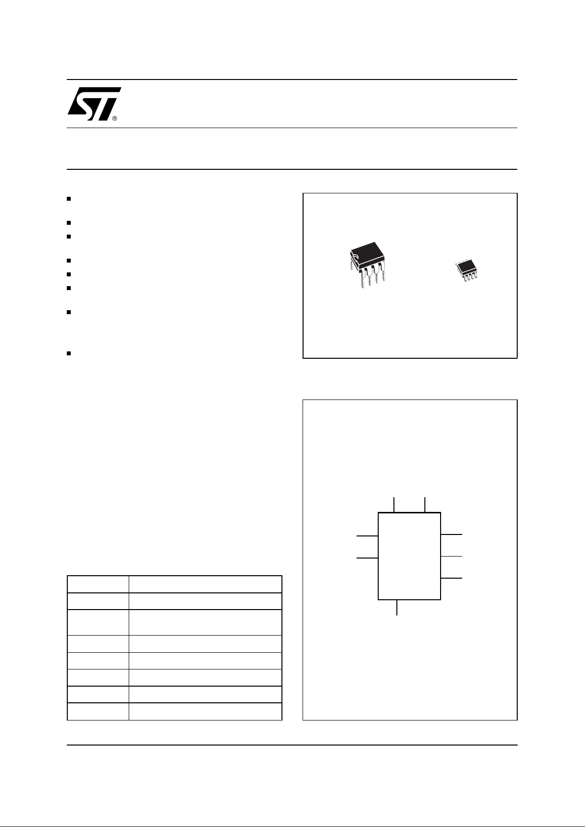
PSDIP8 (N)
0.4mm Frame
MK41T56
MKI41T56
8
1
SO8 (S)
150mil Width
DESCRIPTION
The MK41T56 TIME KEE PE R
®
is a low power 512
bit static CMOS RAM organized as 64 words by 8
bits. A built-in 32.768 kHz oscillator (external crystal
controlled) and the first 8 bytes of the RAM are used
for the clock/calendar function and are configured
in binary coded decimal (BCD) format. Addresses
and data are transferred serially via a two-line
bi-directional bus. The built-in addres s register is
incremented automatically after each write or read
data byte. The MK41T56 clock has a built-in power
sense circuit which detects power failures and
automatically switches to the battery supply during
power failures. The energy needed to sustain the
RAM and clock operations can be supplied from a
small lithium button cell.
T ab le 1. Signal Names
OSCI Oscillator Input
OCSO Oscillator Output
FT/OUT
SDA Serial Data Address Input / Output
SCL Serial Clock
Frequency Test / Output Driver
(Open Drain)
Figure 1. Logic Diagram
V
CC
OSCI
SCL
MK41T56
MKI41T56
V
SS
V
BAT
OSCO
SDA
FT/OUT
AI02304
V
BAT
V
CC
V
SS
March 1999 1/15
Battery Supply Voltage
Supply Voltage
Ground
MK41T56, MKI41T56
Figure 2A. DIP Pin Connections
MK41T56
MKI41T56
OSCI V
1
2
BAT
SS
3
4
V
8
7
6
5
AI02305
FT/OUTOSCO
SCL
SDAV
CC
Figure 2B. SOIC Pin Connections
MK41T56
MKI41T56
OSCI V
1
2
V
BAT
SS
3
4
8
7
6
5
AI02306
FT/OUTOSCO
SCL
SDAV
CC
T ab le 2. Absolute Maximum Ratings
Symbol Parameter Value Unit
T
A
T
STG
V
IO
V
CC
I
O
P
D
Note:
Stresses greater than those listed under "Absolute Maximum Ratings" may cause permanent damage to the device. This is a stress
rating only and functional operation of the device at these or any other conditions above those indicated in the operational section of
this specification is not implied. Exposure to the absolute maximum rating conditions for extended periods of time may affect
reliability.
CAUTION: Negat i ve undershoots below –0.3 volts are not allowed on any pin while in the Battery Back-up mode.
Ambient Operating Temperature MK41T56
MKI41T56
0 to 70
–40 to 85
Storage T emper ature (VCC Off, Oscillator Off) –55 to 125 °C
Input or Output Voltages –0.3 to 7 V
Supply Voltage –0.3 to 7 V
Output Current 20 mA
Power Dissipation 0.25 W
°C
T ab le 3. Register Map
Address
D7 D6 D5 D4 D3 D2 D1 D0
0 ST 10 Seconds Seconds Seconds 00-59
1 X 10 Minutes Minutes Minutes 00-59
2 X X 10 Hours Hours Hour 00-23
3 X X X X X Day Day 01-07
4 X X 10 Date Date Date 01-31
5 X X X 10 M. Month Month 01-12
6 10 Years Years Y ear 00-99
7 OUT FT S Calibration Control
Keys: S
= SIGN Bit; FT = FREQUENCY TEST Bi t; ST = STOP Bi t;
2/15
Data
OUT
= Output level; X = Don’t care.
Function/Range
BCD Format
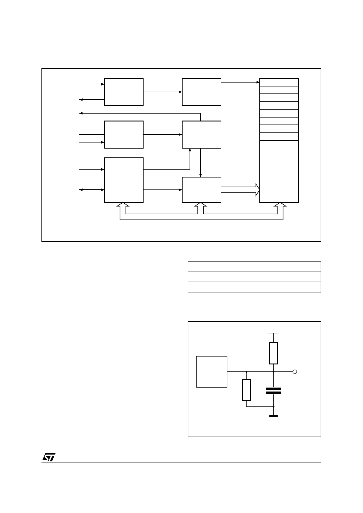
Figure 3. Block Diagram
MK41T56, MKI41T56
OSCI
OSCO
FT/OUT
V
CC
V
SS
V
BAT
SCL
SDA
DESCRIPTION
(cont’d)
OSCILLATOR
32.768 kHz
VOLTAGE
SENSE
and
SWITCH
CIRCUITRY
SERIAL
BUS
INTERFACE
1 Hz
DIVIDER
CONTROL
LOGIC
ADDRESS
REGISTER
SECONDS
MINUTES
HOURS
DAY
DATE
MONTH
YEAR
CONTROL
RAM
(56 x 8)
AI00586C
Table 4. AC Measurement Conditions
Data retention time is in excess of 10 years with a
50mAh 3V lithium cell. The MK41T56 is supplied in
8 pin Plastic Dual-in-Line and 8 lead Plastic SOIC
packages.
OPERATION
The MK41T56 clock operates as a slave dev ice on
the serial bus. Access is obtained by implementing
a start condition followed by the correct slave address (11010000). The 64 bytes contained in the
device can then be ac cessed sequentially in the
following order:
1. Seconds Register
2. Minutes Register
3. Hours Register
4. Day Register
5. Date Register
6. Month Register
7. Years Register
8. Control Register
9 to 64. RAM
Input Rise and Fall Times ≤ 5ns
Input Pulse Voltages 0 to 3V
Input and Output Timing Ref. Voltages 1.5V
Note that Output Hi-Z is defined as the point where data is no
longer driven.
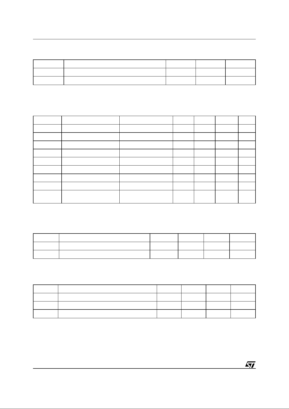
Figure 4. AC Testing Load Circuit
5V
1.8kΩ
DEVICE
UNDER
TEST
1kΩ
CL includes JIG capacitance
OUT
CL = 100pF
AI01019
3/15
MK41T56, MKI41T56
(1,2)
T ab le 5. Capacitance
= 25 °C, f = 1 MHz )
(T
A
Symbol Parameter Min Max Unit
C
IN
(2)
C
OUT
Notes:
1. Effective capacitance measured with power supply at 5V.
2. Sampled, not 100% tested.
3. Outputs deselected.
T ab le 6. DC Characteristics
= 0 to 70°C or –40 to 85°C; VCC = 4.5V to 5.5V)
(T
A
Input Capacitance (SCL) 7 pF
Output Capacitance (SDA, FT/OUT) 10 pF
Symbol Parameter Test Condition Min Typ Max Unit
I
LI
I
LO
I
CC1
I
CC2
V
IL
V
IH
V
OL
V
BAT
I
BAT
Note:
1. The RAYOV AC BR1225 or equivalent is recommended as the battery supply.
Input Leakage Current 0V ≤ VIN ≤ V
Output Leakage Current 0V ≤ V
OUT
≤ V
CC
CC
Supply Current SCL/SDA = VCC–0.3V 1 mA
Supply Current (Standby) 1 mA
Input Low Voltage –0.3 1.5 V
Input High Voltage 3 VCC + 0.8 V
Output Low Voltage IOL = 5mA, VCC = 4.5V 0.4 V
(1)
Battery Supply Voltage 2.6 3 3.5 V
T
= 25°C, VCC = 0V,
Battery Supply Current
A
Oscillator ON, V
BAT
= 3V
450 500 nA
±10 µA
±10 µA
T able 7. Power Down/Up Trip Points DC Characteristics
= 0 to 70°C or –40 to 85°C)
(T
A
(1)
Symbol Parameter Min Typ Max Unit
V
PFD
V
SO
Note:
1. All voltages referenced to V
T ab le 8. Crystal Electrical Characteristics
Power-fail Deselect Voltage 1.2 V
BAT
1.25 V
Battery Back-up Switchover Voltage V
.
SS
BAT
BAT
1.285 V
BAT
(Externally Supplied)
Symbol Parameter Min Typ Max Unit
f
O
R
S
C
Notes:
Load capacitors are integrated within the MK41T56. Cir cuit board layout considerations for the 32.768 kHz crystal of
Resonant Frequency 32.768 kHz
Series Resistance 35 kΩ
Load Capacitance 12.5 pF
L
minimum trace lengths and isolation from RF generating signals should be taken into account.
STMicroelectronics recommends the ECS-.327-12.5-8SP-2 quartz crystal is recommended for industrial temperature operations.
ESC Inc. can be contacted at 800-237-1041 or 913-782-7787 for further information on this crystal type.
V
V
4/15
MK41T56, MKI41T56
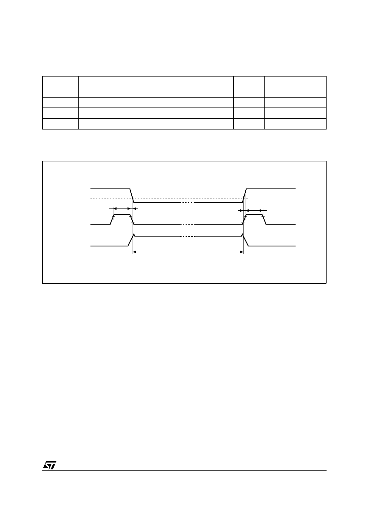
T able 9. Power Down/Up Mode AC Characteristics
= 0 to 70°C or –40 to 85°C)
(T
A
Symbol Parameter Min Max Unit
t
t
t
t
REC
PD
FB
RB
SCL and SDA at VIH before Power Down 0 ns
V
(min) to VSO VCC Fall Time 300 µs
PFD
VSO to V
SCL and SDA at VIH after Power Up 200 µs
(min) VCC Rise Time 100 µs
PFD
Figure 5. Power Down/Up Mode AC Waveforms
V
CC
V
PFD
VSO
SDA
SCL
I
BAT
tPD
tFB
tRB
tREC
DATA RETENTION TIME
OPERATION
The clock continually monitors V
tolerance condition. Should V
(cont’d)
for an out of
CC
fall below V
CC
PFD
the device terminates an access in progress and
resets the device address counter. Inputs to the
device will not be recognized at this time to prevent
erroneous data from being written to the device
from an out of t olerance system. When V
below V
, the device automatically switches over
BAT
CC
falls
to the battery and powers down into an ultra low
current mode of operation to conserve battery life.
Upon power-up, the device switches from battery
to V
at V
CC
goes above V
and recognizes inputs when V
BAT
volts.
PFD
CC
AI00595
2-WIRE BUS CHARACTERISTICS
This bus is intended for communication between
different ICs. It consists of two lines: one bi-direc-
,
tional for data signals (SDA) and one for clock
signals (SCL). Both the SDA and the SCL lines
must be connected to a positive supply voltage via
a pull-up resistor.
The following protocol has been defined:
– Data transfer may be initiated only when the
bus is not busy.
– During data transfer, the data line must remain
stable whenever the clock line is High.
– Changes in the data line while the clock line is
High will be interpreted as control signals.
5/15
 Loading...