

SGS Thomson Microelectronics MJD350, MJD340 Datasheet
MJD340
MJD350
COMPLEMENTARY SILICON POWER TRANSISTORS
■ SGS-THOMSON PREFERRED SALESTYPES
■ COMPLEMENTARYPNP - NPNDEVICES
■ MEDIUMVOLTAGECAPABILITY
■ SURFACE-MOUNTING TO-252 (DPAK)
POWERPACKAGEIN TAPE & REEL
(SUFFIX”T4”)
■ ELECTRICALSIMILARTO MJE340 AND
MJE350
APPLICATIONS
■ SOLENOID/RELAYDRIVERS
■ GENERALPURPOSE SWITCHING AND
AMPLIFIER
DESCRIPTION
The MJD340 and MJD350 form complementary
NPN - PNP pairs.
They are manufactured using Medium Voltage
Epitaxial Planar technology, resulting in a rugged
high performancecost-effectivetransistor.
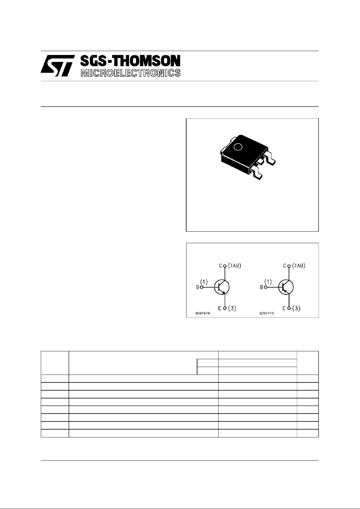
DPAK
TO-252
(Suffix ”T4”)
INTERNAL SCHEMATIC DIAGRAM
3
1
ABSOLUTE MAXIMUM RATINGS
Symb o l Parameter Val ue Uni t
NPN MJD34 0
PNP MJD350
V
V
V
I
P
T
For PNP types voltage and current values are negative.
June 1997
Collect or- B as e Voltage (IE = 0) 300 V
CBO
Collect or- E m it ter Volt age (IB= 0 ) 300 V
CEO
Emitt er-Base Voltage (IC = 0) 3 V
EBO
Collect or Curr en t 0.5 A
I
C
Collect or Peak Current (tp = 2 5oC) 0.75 A
CM
Tot al Power Dissip at ion at T
tot
Stora ge Tempe ra t ur e -65 to 150
stg
Max Oper at ing Junction Temperature 150
T
j
≤ 25oC15W
case
o
C
o
C
1/5
MJD340 / MJD350
THERMAL DATA
R
thj-case
R
thj- amb
Ther mal Resistance Junct ion-cas e Max
Ther mal Resistance Junct ion-ambien t Max
8.33
100
o
C/W
o
C/W
ELECTRICAL CHARACTERISTICS (T
=25oC unlessotherwise specified)
case
Symbol Parameter Test Condition s Min. Typ. Max. Unit
I
CBO
I
EBO
V
CEO(sus)
Collector Cut-off
Current (v
bE
=0)
Emit ter Cut-o f f Current
=0)
(I
C
Collector-Emitt er
=300V 0.1 mA
V
CB
V
=3V 0.1 mA
EB
IC= 1 mA 300 V
Sust aining Voltag e
∗ DC Current G ain IC=50mA VCE=10V 30 240
h
FE
∗
Pulsed: Pulse duration = 300 µs, duty cycle≤ 2%
For PNP type voltage and current values are negative.
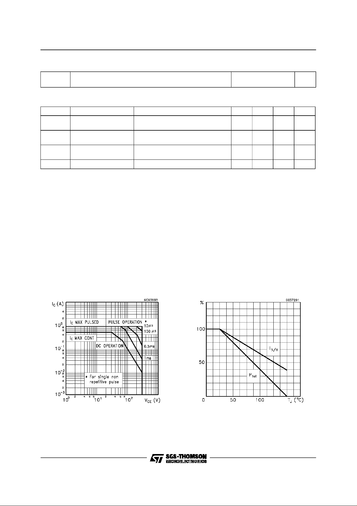
Safe Operating Area DeratingCurve
2/5
 Loading...