

SGS Thomson Microelectronics MJD3055, MJD2955 Datasheet
MJD2955
MJD3055
COMPLEMENTARY SILICON POWER TRANSISTORS
■ STMPREFERRED SALESTYPES
■ SURFACE-MOUNTING TO-252(DPAK)
POWERPACKAGE IN TAPE& REEL
(SUFFIX”T4”)
■ ELECTRICALSIMILARTOMJE2955AND
MJE3055
APPLICATIONS
■ GENERALPURPOSE SWITCHING AND
AMPLIFIERTRANSISTORS
DESCRIPTION
The MJD2955 and MJD3055 form
complementary PNP-NPN pairs. They are
manufacturedusing Epitaxial Base technology for
cost-effectiveperformance.
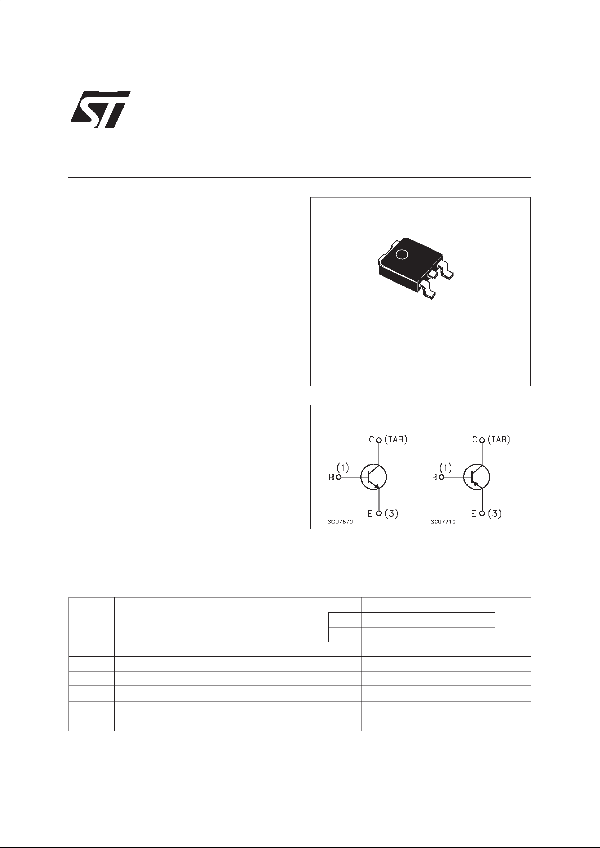
DPAK
TO-252
(Suffix ”T4”)
3
1
INTERNAL SCHEMATIC DIAGRAM
ABSOLUTE MAXIMUM RATINGS
Symb o l Parameter Val u e Uni t
NPN MJD3055
PNP MJD2955
V
V
V
P
Collect or- B as e Voltage (IE=0) 60 V
CBO
Collector-Emitter Voltage (IB=0) 70 V
CEO
Emitter-Base Voltage ( IC=0) 5 V
EBO
I
Collect or Current 10 A
C
I
Base Current 6 A
B
Tot al Di s sipation at Tc=25oC20W
tot
June 1998
1/6
MJD2955 / MJD3055
THERMAL DATA
R
thj-case
R
thj-amb
Ther mal Resistance Junc t io n-c ase Max
Ther mal Resistance Junc t io n-am bien t Max
6.25
100
o
C/W
o
C/W
ELECTRICAL CHARACTERISTICS (T
=25oC unlessotherwise specified)
case
Symbol Parameter Test C ondition s Min. Typ. Max. Unit
I
CEX
I
CBO
I
CEO
I
EBO
V
CEO(sus)
Collector C ut -off
Current
Collector C ut -off
Current (I
E
=0)
Collector C ut -off
Current (I
B
=0)
Emit ter Cut-of f Curr ent
=0)
(I
C
Collector-Emit t er
VCB=70V VBE= -1. 5V
V
=70V VBE= -1. 5V Tj= 150oC
CB
V
=70V
CB
=70V Tj=150oC
V
CB
V
=30V 50 µA
CB
V
=5V 0.5 mA
EB
0.2
2
0.2
2
IC=30mA 60 V
Sust aining V olt ag e
V
∗ Collector-Em itt er
CE(sat)
Saturation Voltage
V
∗ Base-Em itt er V oltage IC=4A VCE=4V 1.8 V
BE(on)
h
∗ DC C urr ent Gain IC=4A VCE=4V
FE
f
∗
Pulsed: Pulse duration = 300 µs, duty cycle1.5 %
For PNP type voltage and currentvalues are negative.
DC C urrent Gain IC=0.5A VCE= 10 V f = 500 KHz 2 MHz
T
IC=4A IB= 0.4 A
I
=10A IB=3.3A
C
I
=10A VCE=4V
C
20
1.1
8
100
5
µA
µA
µA
µA
V
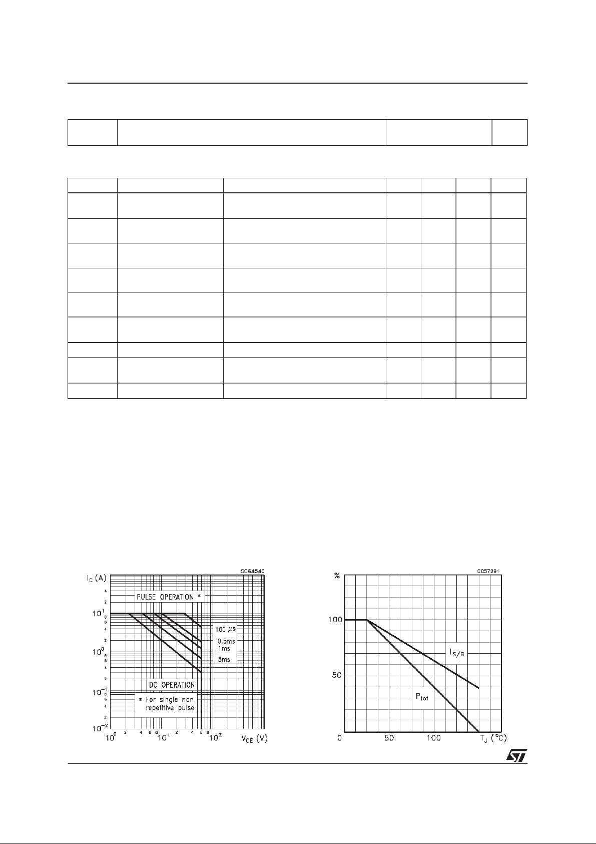
Safe Operating Area DeratingCurves
2/6
 Loading...