

SGS Thomson Microelectronics MJD122T4, MJD127T4, MJD127-1, MJD122-1 Datasheet
MJD122-1 / MJD122T4
MJD127-1 / MJD127T4
COMPLEMENTARY POWER
DARLINGTON TRANSISTORS
Ordering
Code
MJD122T4
MJD122-1
MJD127T4
MJD127-1
■ STMicroelectronics PREFERREDSALESTYPES
■ LOW BASE-DRIVE REQUIREMENTS
■ INTEGRATED ANTIPARALLEL
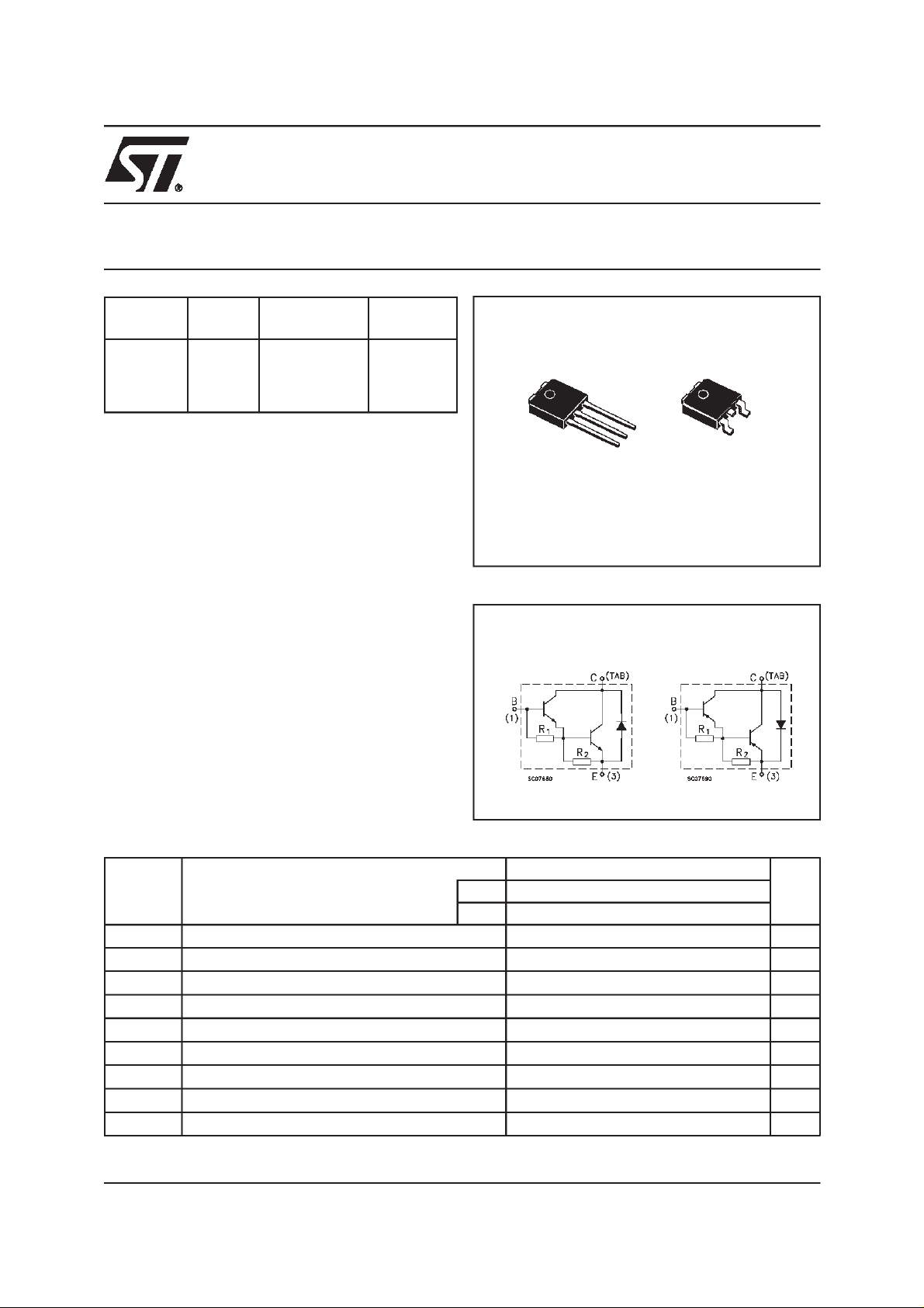
Marking Package Shipment
MJD122
MJD122
MJD127
MJD127
TO-252 (DPAK)
TO-251 (IPAK)
TO-252 (DPAK)
TO-251 (IPAK)
Tape& Reel
Tube
Tape& Reel
Tube
COLLECTOR-EMITTER DIODE
■ THROUGH HOLE TO-251 (IPAK)
POWER PACKAGE IN TUBE (SUFFIX “-1”)
■ SURFACE MOUNTING TO-252 (DPAK)
POWER PACKAGE IN TAPE & REEL
(SUFFIX “T4”)
■ ELECTRICALLY SIMILAR TO TIP122 AND
TIP127
APPLICATIONS:
■ GENERAL PURPOSE SWITCHINGAND
AMPLIFIER
DESCRIPTION
The MJD122 and MJD127 form complementary
NPN - PNP pair. They are manufactured using
Epit axia l B ase tec hnology f or c os t-ef f ect ive
performance.
3
1
TO-251
IPAK
(Suffix ”-1”)
3
2
1
TO-252
DPAK
(Suffix ”T4”)
INTERNAL SCHEMATIC DIAGRAM
Typ. = 150 Ω
R1Typ. = 10 KΩ
R
2
ABSOLUTE MAXIMUM RATINGS
Symbol Parameter Value Unit
NPN MJD122
PNP MJD127
V
CBO
V
CEO
V
EBO
I
I
CM
I
P
T
stg
T
For PNP types voltage and current values are negative.
Collector-Base Voltage (IE=0)
Collector-Emitter Voltage (IB=0)
Emitter-Base Voltage (IC=0)
Collector Current 5 A
C
Collector Peak Current (tp< 5 ms)
Base Current 0.1 A
B
TotalDissipation at Tc=25°C
tot
Storage Temperature –65 to 150 °C
Max. Operating Junction Temperature 150 °C
j
100 V
100 V
5V
8A
20 W
1/8August 2002
MJD122-1 / MJD122T4 / MJD127-1 / MJD127T4
THERMAL DATA
R
thj-case
R
thj-amb
ELECTRICAL CHARACTERISTICS (Tj=25°C unless otherwise specified)
Symbol Parameter Test Conditions Min. Typ. Max. Unit
I
CBO
I
CEO
I
CEX
I
EBO
V
CEO(sus)
V
CE(sat)
V
BE(sat)
V
BE(on)
h
FE
* Pulsed: Pulse duration = 300 µs, duty cycle ≤ 2%.
For PNP types voltage and current values are negative.
Thermal Resistance Junction-case
Thermal Resistance Junction-ambient
Collector Cut-off
Current (I
E
=0)
Collector Cut-off
Current (I
B
=0)
Collector Cut-off
Current (V
= -1.5 V)
BE
Emitter Cut-off Current
(I
=0)
C
* Collector-Emitter
= 100 V 10 µA
V
CB
=50V 10 µA
V
CE
= 100 V
V
CE
= 100 V
V
CE
=5V 2 mA
V
EB
= 30 mA 100 V
I
C
Sustaining Voltage
(I
=0)
B
* Collector-Emitter
Saturation Voltage
* Base-Emitter
IC=4A
=8A
I
C
IC=8A IB= 80 mA 4.5 V
Saturation Voltage
* Base-Emitter On
IC=4A VCE= 4 V 2.8 V
Voltage
* DC Current Gain IC=4A
=8A
I
C
T
=125°C
j
I
=16mA
B
=80mA
I
B
V
=4V
CE
=4V
V
CE
Max
Max
1000
100
6.25
100
10
500µAµA
2
4
12000
°C/W
°C/W
V
V
2/8
MJD122-1 / MJD122T4 / MJD127-1 / MJD127T4
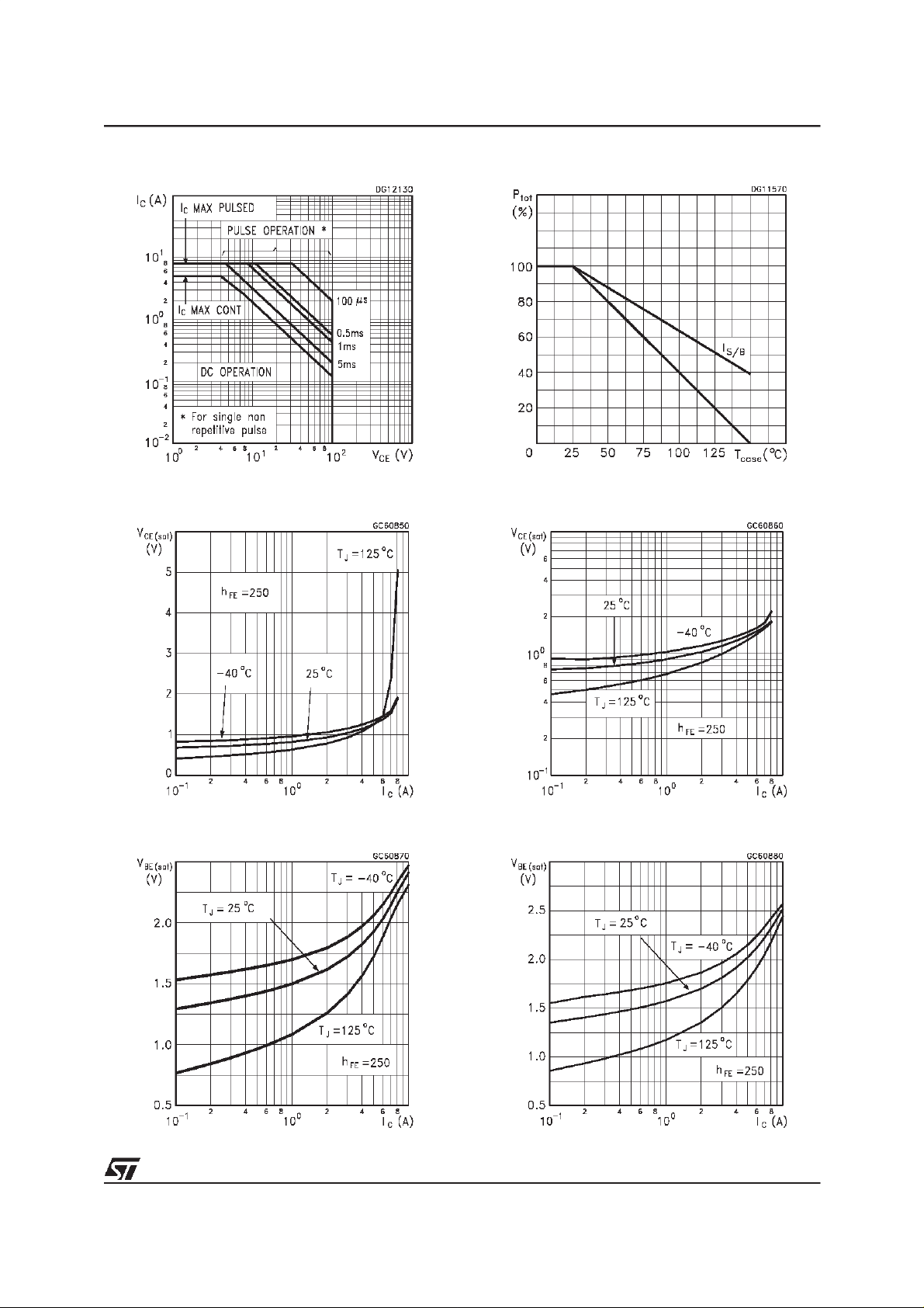
Safe Operating Area Derating Curve
Collector-Emitter Saturation Voltage (PNP type)Collector-Emitter Saturation Voltage (NPN type)
Base-Emitter Saturation Voltage (NPN type)
Base-Emitter Saturation Voltage (PNP type)
3/8
 Loading...