

SGS Thomson Microelectronics MJB32B Datasheet
®
PNP SILICON POWER TRANSISTOR
■ SURFACE-MOUNT ING D
POWER PACKAGE IN TAPE & REEL
(SUFFIX "T4")
■ ELECTRICALLY SIMILAR TO TIP32B
APPLICATION
■ LINEAR AND SWITCHING INDUSTRIAL
EQUIPMENT
DESCRIPTION
The MJB32B is manufactured using
Epitaxial-base Technology for use in medium
power linear and switching applications.
2
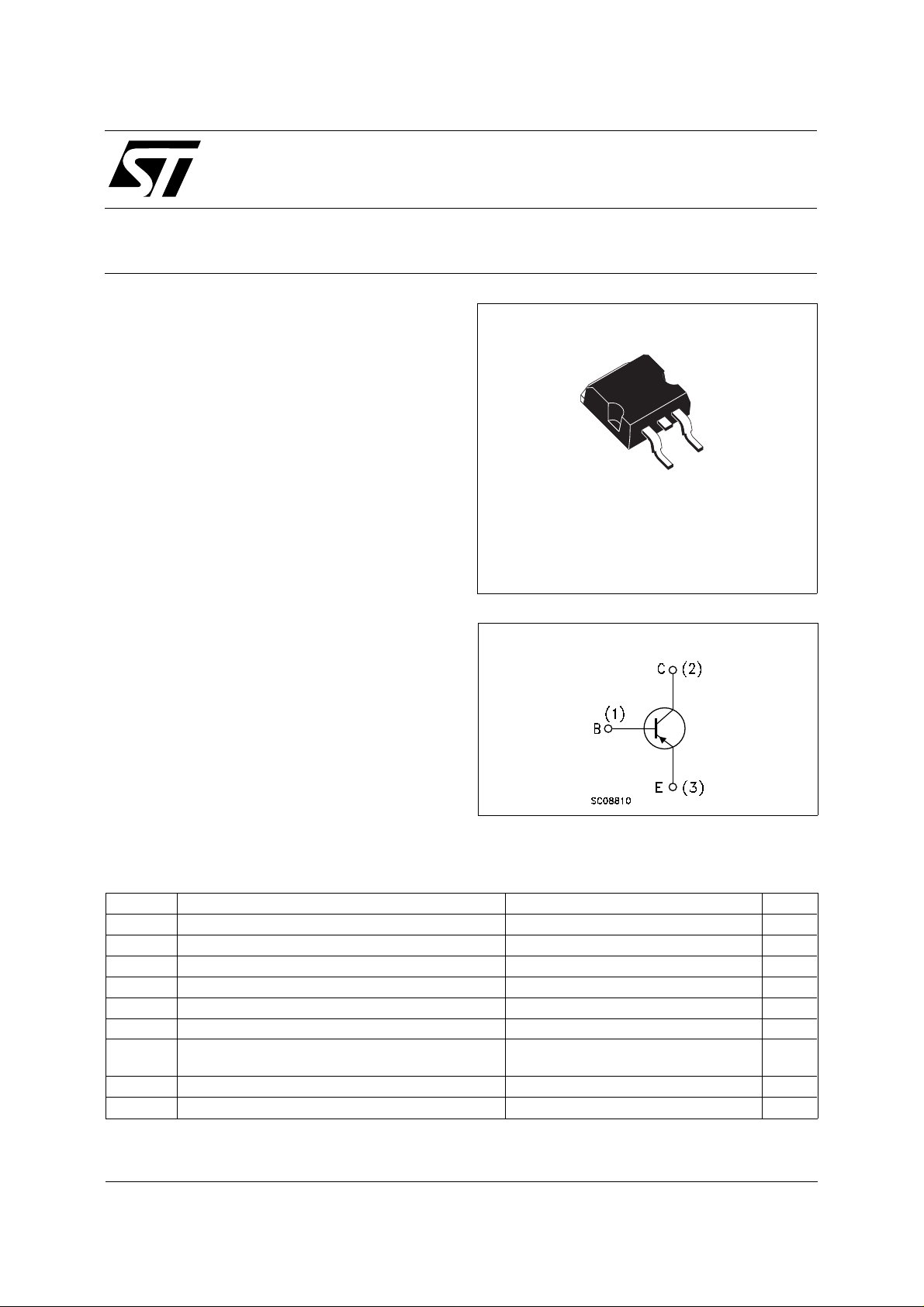
PAK (TO-263)
MJB32B
3
1
D2PAK
(TO-263)
(Suffix "T4")
INTER NAL SCH E M ATI C DIAG RA M
ABSOLUTE MAXIMUM RATINGS
Symbol Parameter Value Unit
V
V
V
I
P
T
Collector-Base Voltage (IE = 0) -80 V
CBO
Collector-Emitter Voltage (IB = 0) -80 V
CEO
Emitter-Base Voltage (IC = 0) -5 V
EBO
Collector Current -3 A
I
C
Collector Peak Current -5 A
CM
Base Current -1 A
I
B
Total Dissipation at T
tot
T
Storage Temperature -65 to 150
stg
T
Max. Operating Junction Temperature 150
j
case
amb
≤ 25 oC
≤ 25 oC
40
2
W
W
o
C
o
C
June 2001
1/5
MJB32B
THERMAL DATA
R
thj-case
R
thj-amb
Thermal Resistance Junction-case Max
Thermal Resistance Junction-ambient Max
3.12
62.5
o
C/W
o
C/W
ELECTRICAL CHARACTERISTICS (T
= 25 oC unless otherwise specified)
case
Symbol Parameter Test Conditions Min. Typ. Max. Unit
I
CEO
I
CES
I
EBO
V
CEO(sus)
Collector Cut-off
Current (I
= 0)
B
Collector Cut-off
Current (V
BE
= 0)
Emitter Cut-off Current
(I
= 0)
C
∗ Collector-Emitter
= -60 V -50 µA
V
CE
= -80 V -20 µA
V
CE
= -5 V -0.1 mA
V
EB
I
= -30 mA -80 V
C
Sustaining Voltage
(I
= 0)
B
∗ Collector-Emitter
V
CE(sat)
IC = -3 A IB = -375 mA -1.2 V
Saturation Voltage
V
∗ Base-Emitter Voltage IC = -3 A VCE = -4 V -1.8 V
BE
hFE∗ DC Current Gain IC = -1 A VCE = -4 V
I
= -3 A VCE = -4 V
C
h
∗ Pulsed : pulse duration = 300 µs, duty cycle ≤ 2%
Small Signall Current
fe
Gain
IC = -0.5 A VCE = -10 V f = 1 KHz
I
= -0.5 A VCE = -10 V f = 1 MHz
C
25
10 50
20
3
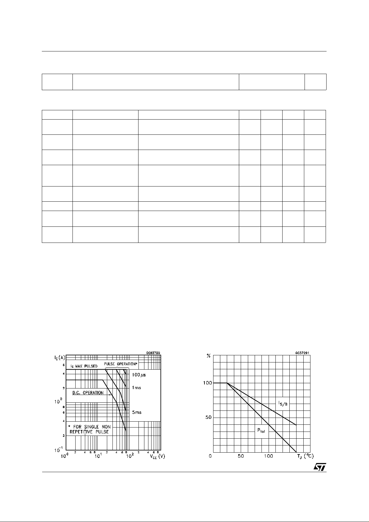
Safe Operating Are a Derating Curves
2/5
 Loading...