

SGS Thomson Microelectronics MC35172DT, MC35172N, MC35172D, MC35172 Datasheet
1
2
3
45
6
7
8
-
+
-
+
Ouptut
Inverting Input 2
Non-inverting Input 2
Inverting Input 1
Output 1
Non-inverting Input 1
V
CC
V
CC
MC33172 - MC35172
LOW POWER
DUAL BIPOLAR OPERATIONAL AMPLIFIERS
■ GOOD CONSUMPTI ON/SPEED RATIO :
ONLY 200µA FOR 2.1MHz, 2Vµs
■ SINGLE (OR DUAL) SUPPLY OPERATION
FROM +4V TO +44V (±2V TO ±22V)
■ WIDE INPUT COMMON MODE MODE
VOLTAGE RANGE INCLUDING V
CC
-
■ LOW LEVEL OUTPUT VOLTAGE CLOSE TO
-
: 100mV TYPICAL
V
CC
■ PIN TO PIN COMPATIB LE WITH
STANDARD DUAL OP-AMPs
DESCRIPTION
The MC3x172 series are dual bipolar operationa l
amplifiers offering bot h low consumption (200µA/
Amp) and good speed (2.1MHz, 2V/µs).
Moreover the Input Common Mode Range extends down to the lower supply rail, allowing single
supply operation from +4V to +44V.
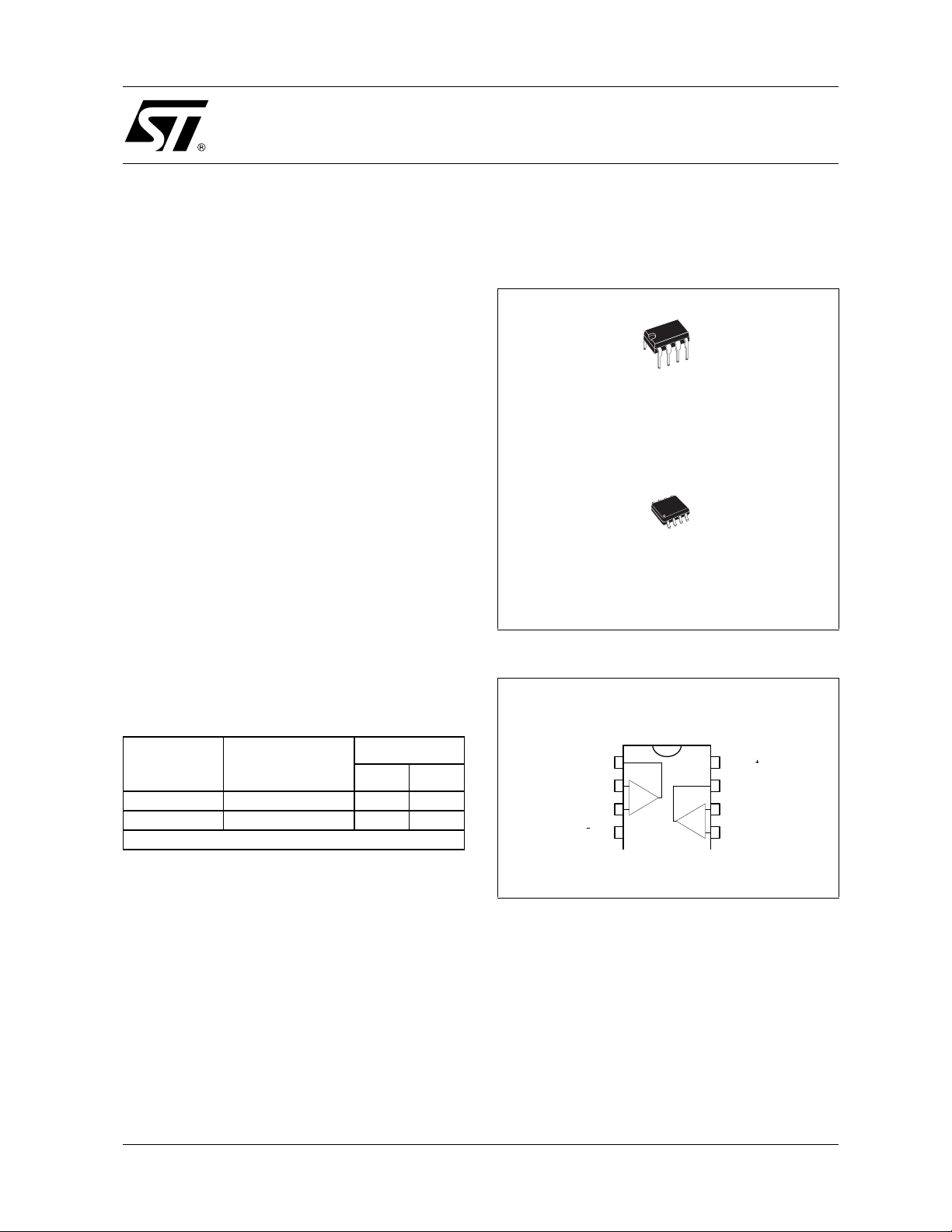
N
DIP8
(Plastic Package)
D
SO8
(Plastic Micropacka ge)
PIN CONNECTIONS (top view)
ORDER CODE
Part Number
MC33172 -40°C, +105°C
MC35172 -55°C, +125°C
Example : MC33172N
N = Dual in Line Package (DIP)
D = Small Outline Package (SO) - also available in Tape & Reel (DT))
November 2001
Temperature
Range
Package
ND
••
••
1/5
MC33172-MC35172
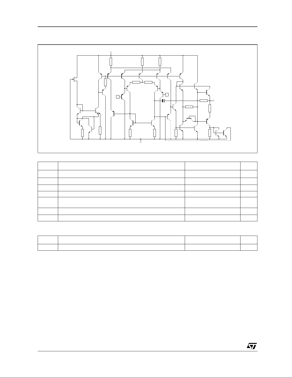
SCHEMATIC DIAGRAM (for 1/2MC33172)
V +
CC
R4
T8
T1
T2
T3
R1
T7
T5
T4
R2
T9
R3
T6
Input -
T14
T13
R5
R7
T15
T19
R9
V -
CC
R6
T13
T10
T11
R8
T16
T20
R10
T12
T25
Input +
T17
C
T21
T24
R12
T22
T27
T23
R11
T26
R13
Output
R14
T28
T29
R15
T30
T31
MAXIMUM RATINGS
Symbol Parameter Value Unit
V
T
T
1. Either or both input voltages must not exceed the magnitude of Vcc.
Supply Voltage ±22 V
CC
V
Differential Input Voltage
id
V
Input Voltage see note 1 V
i
see note
Output Short Circuit Duration Indefinite s
Operating Free-Air Temperature range MC33172
oper
MC35172
T
Junction Temperature 150 °C
j
Storage Temperature -65 to 150 °C
stg
-40 to 105
-55 to 125
1)
V
°C
OPERATING CONDITIONS
Symbol Parameter Value Unit
V
2/5
Supply Voltage ±2 to ±22 V
CC
 Loading...