

LOW NOISE QUAD OPERATIONAL AMPLIFIERS
.
LOW VOLTAGE NOISE: 4.5nV/√√Hz
.
HIGHGAIN BANDWIDTHPRODUCT: 15MHz
.
HIGHSLEW RATE : 7V/µµs
.
LOW DISTORTION : 0.002%
.
LARGE OUTPUT VOLTAGE SWING :
+14.3V/-14.6V
.
EXCELLENTFREQUENCY STABILITY
.
ESD INTERNALPROTECTION
.
MACROMODEL INCLUDED IN THIS
SPECIFICATION
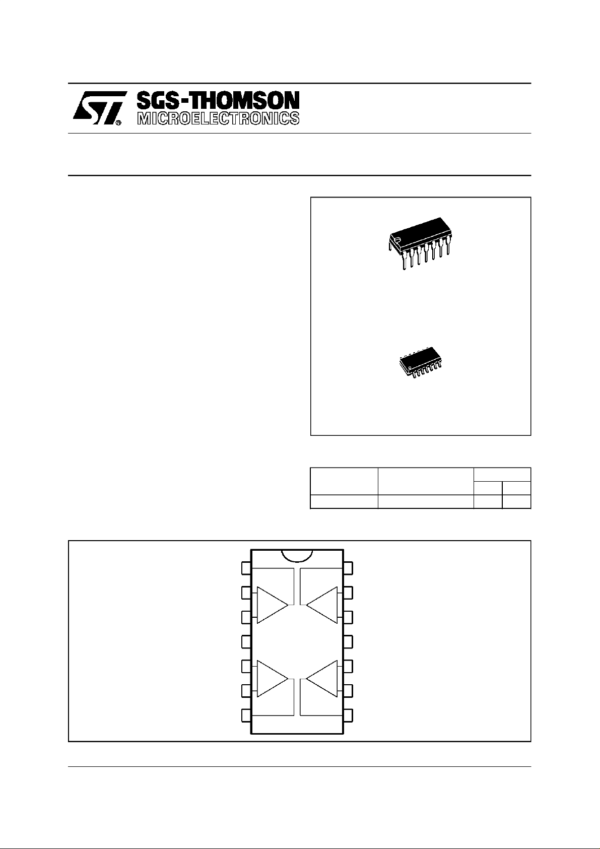
MC33079
N
DIP14
(Plastic Package)
DESCRIPTION
The MC33079 is a monolithic quad operational
amplifier particularly well suited for audio applications. It offerslow voltage noise (4.5nV/√Hz ) and
high frequencyperformances (15MHzGain Bandwidth product, 7V/µsslew rate).
In addition the MC33079has a verylow distortion
(0.002%)and excellentphase/gainmargins.
The output stage allows a large output voltage
swing andsymmetrical source and sink currents.
PIN CONNECTIONS (top view)
CC
1
2
3
+
4
5
-
+
+
Output 1
Inverting Input 1
Non-inverting Input 1
V
Non-inverting Input 2
D
SO14
(Plastic Micropackage)
ORDER CODES
Part Number Temperature Range
o
MC33079 -40, +105
14
Output 4
13
-
+
+
Inverting Input 4
12
Non-inverting Input 4
-
V
11
CC
10
Non-inverting Input 3
C ••
Package
ND
November 1997
Inverting Input 2
Output 2
6
7
-
-
9
Inverting Input 3
8
Output 3
1/9
MC33079
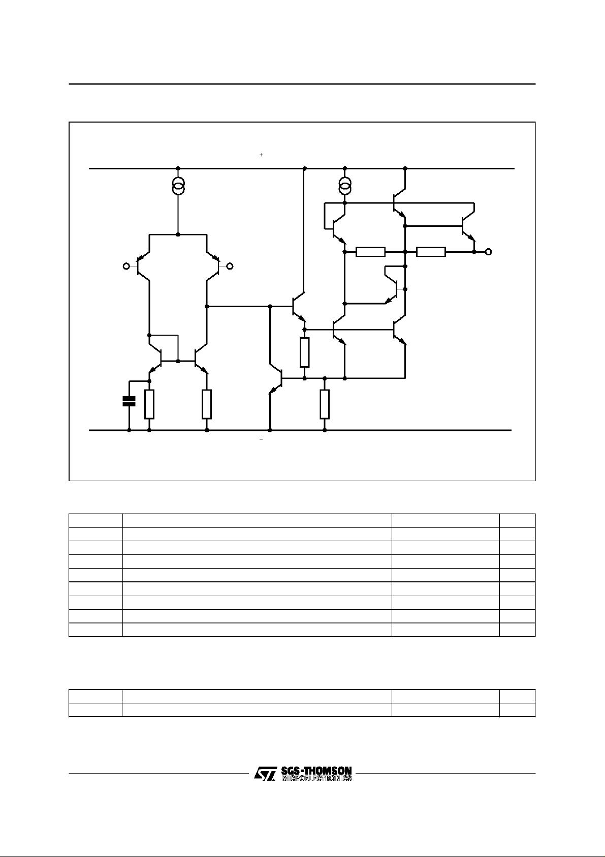
SCHEMATIC DIAGRAM (1/4MC33079)
V
CC
Inverting
Input
Non-inve rting
Input
V
CC
ABSOLUTEMAXIMUMRATINGS
Symbol Parameter Value Unit
Output
V
CC
V
id
V
T
oper
T
T
stg
P
tot
Notes : 1. Either or both input voltages mustnotexceed the magnitude of V
Supply Voltage ±18 or +36 V
Differential Input Voltage - (note 1) ±30 V
Input Voltage- (note 1) ±15 V
i
Output Short-Circuit Duration - (note 2) Infinite
Operating Free-air Temperature Range -40 to +105
Maximum Junction Temperature +150
j
Storage Temperature -65 to +150
Maximum Power Dissipation - (note 2) 500 mW
+
-
or V
CC
2. Power dissipation must be considered to ensure maximum junction temperature (Tj) is not exceeded
CC
o
C
o
C
o
C
OPERATINGCONDITIONS
Symbol Parameter Value Unit
Supply Voltage ±2.5 to ±15 V
2/9
V
CC
MC33079
ELECTRICAL CHARACTERISTICS
+
= +15V,V
V
CC
Symbol Parameter Min. Typ. Max. Unit
V
io
DV
io
I
io
I
ib
V
icm
A
vd
±V
opp
CMR Common Mode Rejection Ratio (V
SVR SupplyVoltage RejectionRatio
I
o
I
CC
SR Slew Rate
GBP Gain Bandwidth Product (f = 100kHz, R
B Unity Gain Bandwidth (Open loop) 9 MHz
A
m
∅m Phase Margin (R
e
n
i
n
THD Total Harmonic Distortion
V
O1/VO2
FPB Full Power Bandwidth (V
Z
o
R
i
C
i
-
= -15V,T
CC
Input Offset Voltage (Vo= 0V, Vic= 0V)
≤ T
T
min.
amb
=25oC (unlessotherwisespecified)
amb
≤ T
max.
2.5
3.5
Input Offset Voltage Drift
= 0V, Vo= 0V, T
V
ic
min.
≤ T
amb
≤ T
max.
2
Input Offset Current (Vic=0V,VO= 0V)
T
T
amb
min.
= +25oC
≤ T
amb
≤ T
max.
10 150
175
Input Bias Current (Vic= 0V, VO= 0V)
T
T
amb
min.
= +25oC
≤ T
amb
≤ T
max.
250 750
800
Common Mode Input Voltage Range (∆VIO= 5mV, VO= 0V) ±13 ±14 V
Large Signal Voltage Gain (RL=2kΩ,VO=±10V)
T
T
amb
min.
= +25oC
≤ T
amb
≤ T
max.
90
85
100
Output Voltage Swing (Vid= ±1V)
= 600Ω
R
L
= 600Ω
R
L
R
= 2.0kΩ
L
= 2.0kΩ
R
L
R
= 10kΩ
L
= 10kΩ
R
L
= ±13V) 80 100 dB
ic
+
-
/V
V
CC
= +15V / -15V to +5V / -5V 80 105
CC
13.2
13.5
12.2
-12.7
14
-14.2
14.3
-14.6
-13.2
-14
Output Short Circuit Current (Vid= ±1V, Output to Ground)
Source
Sink
15
20
29
37
Supply current (VO= 0V, All Amplifiers)
= +25oC
T
amb
≤ T
T
min.
= -10Vto +10V, RL=2kΩ,CL= 100pF, AV=+1 5 7
V
i
Gain Margin(RL=2kΩ)C
≤ T
amb
max.
=2kΩ,CL= 100pF) 10 15 MHz
L
L
C
L
=2kΩ)C
L
L
C
L
= 0pF
= 100pF
= 0pF
= 100pF
810
12
-11
-6
55
30
Equivalent Input Noise Voltage (RS= 100Ω, f = 1kHz) 4.5
Equivalent Input Noise current (f = 1kHz) 0.5
=2kΩ, f = 20Hz to 20kHz, VO=3V
R
L
= +1 0.002
rms,AV
Channel Separation (f = 20Hz to 20kHz) 120 dB
= 27Vpp,RL=2kΩ, THD ≤ 1%) 120 kHz
O
Output Impedance (VO= 0V, f = 9MHz) 37 Ω
Input Resistance (Vic= 0V) 175 kΩ
Input Capacitance (Vic= 0V) 12 pF
mV
o
µV/
C
nA
nA
dB
V
dB
mA
mA
V/µs
dB
Degrees
nV
Hz
√
pA
Hz
√
%
3/9

MC33079
SUPPLY CURRENT vs SUPPLY VOLTAGE
10
8
6
4
Supply Current (mA)
2
0
0 5 10 15 20 25 30
Supply Voltage(V)
OUTPUT VOLTAGE vs SUPPLY VOLTAGE
15
10
5
0
-5
Output Voltage (V)
-10
-15
0 5 10 15
Supply Voltage (V)
Vid=±1V
RL=600ohms
OUTPUT SHORT CIRCUIT CURRENT vs
OUTPUT VOLTAGE
60
40
20
0
-20
Output ShortCircuit Current (mA)
-40
0 102030
Vcc=0/30V
Tamb.=25°C
Output Voltage(V)
OUTPUT VOLTAGEvs SUPPLYVOLTAGE
15
10
5
0
-5
Output Voltage (V)
-10
-15
0 5 10 15
SupplyVoltage (V)
Vid=±1V
RL=2kohms
EQUIVALENT INPUT NOISE VOLTAGE vs
FREQUENCY
10
4/9
8
6
4
2
Equivalent Input Noise Voltage (nV/VHz)
0
0,01 0,1 1 10 100 1000
Vcc=±15V Av=100
Rs=100ohms Tamb.=25°C
Frequency (kHz)
THD + NOISE vsFREQUENCY
0,01
RL=2kohms Vo=3Vrms
Vcc=±15V
0,005
THD+Noise(%)
0
0,01 0,1 1 10 100
Frequ ency (kHz)
Gain= 10
Gain= 1

MC33079
VOLTAGEGAIN AND PHASEvs FREQUENCY
60
40
20
0
Gain (dB)
-20
-40
10 100 1000 10000 100000
RL=2kohms CL=100pF
Frequency (kHz)
Vcc=±15V Av=-100
180
120
60
0
-60
-120
Phase (Deg)
TOTALHARMONIC DISTORTIONvs OUTPUT
VOLTAGE
0,020
0,015
0,010
THD+Noise(%)
0,005
0,000
RL=2kohms F=1kHz
Vcc=±15V Av= 10
0123456789
Vout(Vrms)
5/9

MC33079
MACROMODEL
.
LOW VOLTAGENOISE : 4.5nV/√√Hz
.
HIGHGAIN BANDWIDTHPRODUCT: 15MHz
.
HIGHSLEW RATE : 7V/µµs
.
LOW DISTORTION : 0.002%
.
LARGE OUTPUT VOLTAGE SWING :
+14.3V/-14.6V
.
EXCELLENTFREQUENCY STABILITY
.
ESD INTERNALPROTECTION
** StandardLinear Ics Macromodels,1993.
** CONNECTIONS :
* 1 INVERTING INPUT
* 2 NON-INVERTING INPUT
* 3 OUTPUT
* 4 POSITIVEPOWER SUPPLY
* 5 NEGATIVE POWERSUPPLY
.SUBCKTMC33079 1 3 2 4 5(analog)
********************************************************
**
.MODEL MDTH D IS=1E-8 KF=2.286238E-16
CJO=10F
* INPUTSTAGE
CIP 2 5 1.200000E-11
CIN 1 5 1.200000E-11
EIP 10 5 2 5 1
EIN 16 51 51
RIP 10 112.363636E+00
RIN 15 16 2.363636E+00
RIS 1115 1.224040E+01
DIP 1112 MDTH 400E-12
DIN 15 14 MDTH 400E-12
VOFP12 13 DC0
VOFN 13 14 DC 0
IPOL 13 5 1.100000E-04
CPS 11 15 2.35E-09
DINN 17 13 MDTH 400E-12
VIN 17 51.000000e+00
DINR 15 18 MDTH 400E-12
VIP 4 18 1.000000E+00
FCP4 5VOFP1.718182E+01
FCN 5 4VOFN 1.718182E+01
FIBP2 5VOFN4.545455E-03
FIBN 5 1 VOFP4.545455E-03
* AMPLIFYINGSTAGE
FIP 519 VOFP 9.545455E+02
FIN 5 19 VOFN 9.545455E+02
CC 19 29 1.500000E-08
HZTP30 29 VOFP1.523529E+02
HZTN 5 30 VOFN1.523529E+02
DOPM51 22 MDTH400E-12
DONM 21 52 MDTH400E-12
HOPM22 28 VOUT5.172414E+03
VIPM28 41.500000E+02
HONM 21 27 VOUT4.054054E+03
VINM 5 27 1.500000E+02
DBIDON119 53 MDTH 400E-12
V1 51 53 0.68
DBIDON254 19 MDTH 400E-12
V2 54 52 0.68
RG1151 5 3.04E+05
RG1251 4 3.04E+05
RG2152 5 0.6072E+05
RG2252 4 0.6072E+05
E1 50 40 51 0 1 E240 39 52 0 1
EDEC1 38 39 4 0 0.5
EDEC2 0 38 5 0 0.5
DOP 51 25 MDTH400E-12
VOP4 25 1.474575E+00
DON 24 52 MDTH400E-12
VON 24 5 1.474575E+00
RAJUS50 5 1E12
GCOMP 5 4 4 5 8.1566068E-04
RPM1 5 80 1E+06
RPM2 4 80 1E+06
GAVPH5 82 5080 3.26E-03
RAVPHGH 82 4 613
RAVPHGB 825 613
RAVPHDH 82 83 1000
RAVPHDB 82 84 1000
CAVPHH 4 83 0.159E-09
CAVPHB 5 84 0.159E-09
EOUT26238251
VOUT23 5 0
ROUT 26 3 4.780354E+01
COUT 3 5 1.000000E-12
.ENDS
6/9

ELECTRICALCHARACTERISTICS
V
CC
+
= +15V, V
CC
-
= -15V, T
=25oC, (unlessotherwise specified)
amb
Symbol Conditions Value Unit
V
io
A
vd
I
CC
V
icm
V
opp
I
sink
I
source
GBP R
SR R
∅mR
RL=2kΩ,Vo=±10V 100 dB
No load, per operator 2 mA
∆Vio= 5mV, Vo=0V 28 V
RL=2kΩ 28.2 V
VO=0V 37 mA
VO=0V 29 mA
=2k
L
=2k
L
=2k
L
Ω,
CL= 100pF 15 MHz
Ω,
CL= 100pF, AV=+1 7 V/µs
Ω,
CL= 0pF 55 Degrees
0mV
MC33079
7/9

MC33079
PACKAGE MECHANICALDATA
14 PINS- PLASTICDIP
Dimensions
Min. Typ. Max. Min. Typ. Max.
Millimeters Inches
a1 0.51 0.020
B 1.39 1.65 0.055 0.065
b 0.5 0.020
b1 0.25 0.010
D 20 0.787
E 8.5 0.335
e 2.54 0.100
e3 15.24 0.600
F 7.1 0.280
i 5.1 0.201
L 3.3 0.130
Z 1.27 2.54 0.050 0.100
PM-DIP14.EPS
DIP14.TBL
8/9

PACKAGE MECHANICALDATA
14 PINS- PLASTICMICROPACKAGE (SO)
MC33079
Dimensions
Min. Typ. Max. Min. Typ. Max.
Millimeters Inches
A 1.75 0.069
a1 0.1 0.2 0.004 0.008
a2 1.6 0.063
b 0.35 0.46 0.014 0.018
b1 0.19 0.25 0.007 0.010
C 0.5 0.020
c1 45
o
(typ.)
D 8.55 8.75 0.336 0.334
E 5.8 6.2 0.228 0.244
e 1.27 0.050
e3 7.62 0.300
F 3.8 4.0 0.150 0.157
G 4.6 5.3 0.181 0.208
L 0.5 1.27 0.020 0.050
M 0.68 0.027
S8
Information furnished is believed tobe accurate andreliable. However, SGS-THOMSON Microelectronics assumes no responsibility
for the consequences of useof suchinformation nor for any infringement of patentsor other rights of third parties whichmay result
from itsuse. No license is granted byimplication or otherwiseunder anypatent or patent rights ofSGS-THOMSON Microelectronics.
Specification mentioned in this publication are subject to change without notice. This publication supersedes and replaces all
information previously supplied.SGS-THOMSON Microelectronics products are not authorized for useas critical components in life
support devices or systems withoutexpress written approval of SGS-THOMSON Microelectronics.
o
(max.)
SO14.TBL
1997 SGS-THOMSON Microelectronics – Printed in Italy – AllRights Reserved
SGS-THOMSON Microelectronics GROUPOF COMPANIES
Australia- Brazil - Canada - China - France- Germany - Italy - Japan - Korea - Malaysia - Malta - Morocco
The Netherlands - Singapore - Spain - Sweden - Switzerland - Taiwan- Thailand -United Kingdom - U.S.A.
ORDER CODE : PM-SO14.EPS
9/9
 Loading...