

Datasheet M93S56-MN3, M93S56-BN6, M93S56-BN3, M93S46-MN6, M93S46-MN3 Datasheet (SGS Thomson Microelectronics)
...
M93S66, M93S56, M93S46
4K/2K/1K (x16) Serial Microwire Bus EEPROM
with Block Protection
February 1999 1/23
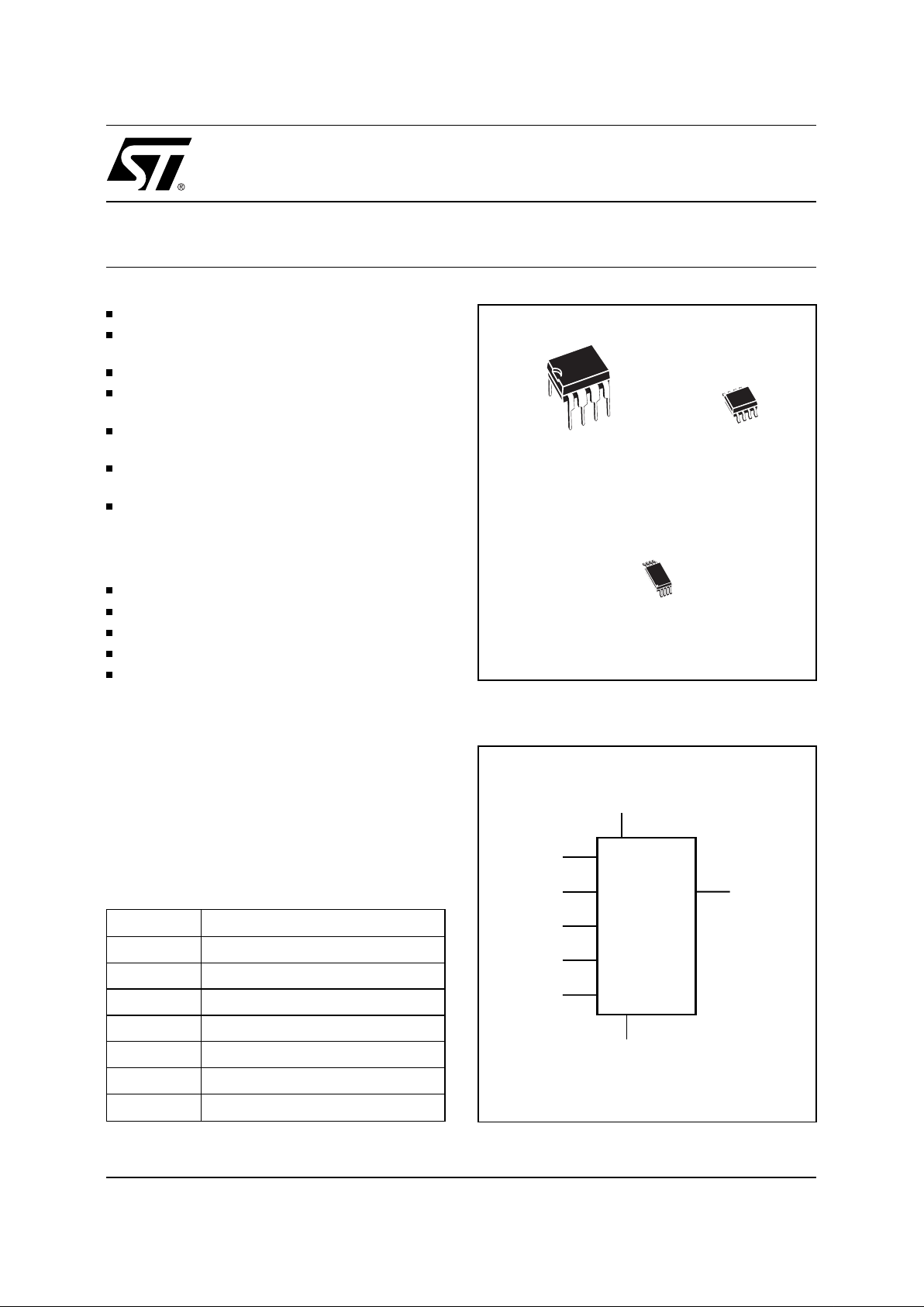
AI02020
D
V
CC
M93Sx6
V
SS
C Q
PRE
W
S
Figure 1. Logic Diagram
INDUSTRY STANDARD MICROWIRE BUS
1 MILLION ERASE/WRITE CYCLES, with
40 YEARS DATA RETENTION
SINGLE ORGANIZATION by WORD (x16)
WORD and ENTIRE MEMORY
PROGRAMMING INSTRUCTION S
SELF-TIMED PROGRAMMING CY CLE with
AUTO-ERASE
READY/BUSY SIGNAL DURING
PROGRAMMING
SINGLE SUPPLY VOLTAGE:
– 4.5V to 5.5V for M9 3Sx6 version
– 2.5V to 5.5V for M93Sx6-W version
– 1.8V to 3.6V for M93Sx6-R version
USER DEFINED WRITE PROTE CT ED AREA
PAGE WRITE MODE (4 words)
SEQUENTIAL READ OPERATION
5ms TYPICAL PROGRAMMING TIME
ENHANCED ESD and LATCH-UP
PERFORMANCES
DESCRIPTION
This M93S46/S56/S66 specification covers a
range of 4K/2K/1K bit serial EEPROM products
respectively . In this text, products are referred to as
M93Sx6. The M93Sx6 is an Electrically Erasable
Programmable Memory (EEPROM) fabricated with
STMicroelectronics’s High Endurance Single
Polysilicon CMOS technology .
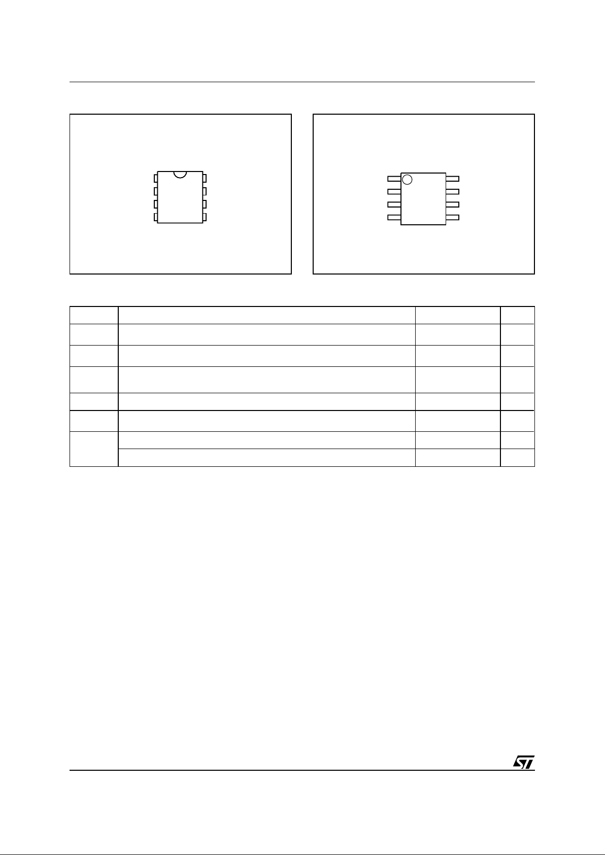
S Chip Select Input
D Serial Data Input
Q Serial Data Output
C Serial Clock
PRE Protect Enable
W Write Enable
V
CC
Supply Voltage
V
SS
Ground
T ab le 1. Signal Names
8
1
SO8 (MN)
150mil Width
8
1
PSDIP8 (BN)
0.25mm Frame
8
1
TSSOP8 (DW)
169mil Width
The M93Sx6 memory is ac ces sed through a ser ial
input (D) and output (Q) using the MICROWIRE
bus protocol. The M93Sx6 is specified at 5V ±10%,
the M93Sx6-W specified at 2.5V to 5.5V and the
M93Sx6-R specified at 1.8V to 3.6V.
The M93S66/S56/S46 memory is divided into
256/128/64 x16 bit words respectively. These
memory devices are available in both PSDIP8,
SO8 and TSSOP8 packages.
The M93Sx6 memory is accessed by a set of
instructions which includes Read, Write, Page
V
SS
Q
W
PREC
SV
CC
D
AI02021
M93Sx6
1
2
3
4
8
7
6
5
Figure 2A. DIP Pin Connections
1
V
SS
Q
W
PREC
SV
CC
D
AI02022
M93Sx6
2
3
4
8
7
6
5
Figure 2B. SO and TSSOP Pin Connections
DESCRIPTION (cont’d) Write, Write All and instructions used to set the
memory protection. A Read instruction loads the
address of the first word to be read into an internal
address pointer . The data contained at this address
is then clocked out serially. The address pointer is
automatically incremented after the data is output
and, if the Chip Select input (S) is held High, the
M93Sx6 can output a sequential stream of data
words. In this way, the memory can be read as a
data stream from 16 to 4096 bits (for the M93S66),
or continuously as the address counter automatically rolls over to ’00’ when the highest address is
reached.
Symbol Parameter Value Unit
T
A
Ambient Operating Temperature –40 to 125
°
C
T
STG
Storage Temperature –65 to 150
°
C
T
LEAD
Lead T e mperature, Soldering (SO8 package)
(PSDIP8 package)
40 sec
10 sec
215
260
°
C
V
IO
Input or Output Voltages (Q = VOH or Hi-Z) –0.3 to VCC +0.5 V
V
CC
Supply Voltage –0.3 to 6.5 V
V
ESD
Electrostatic Discharge Voltage (Human Body model)
(2)
4000 V
Electrostatic Discharge Voltage (Machine model)
(3)
500 V
Notes:
1. Except for the rating "Operating Temperature Range", stresses above those listed in the Table "Absolute Maximum Ratings"
may cause permanent damage to the device. These are stress rating s only and operation of the device at these or any other
conditions above those indicated in the Operating sections of this specification is not implied. Exposure to Absolute Maximum
Rating conditions for extended periods may affect device reliability. Refer also to the STMicroelectronics SURE Program and other
relevant quality documents.
2. MIL-STD-883C, 3015.7 (100pF, 1500 Ω).
3. EIAJ IC-121 (Condition C) (200pF, 0 Ω).
T ab le 2. Absolute Maximum Ratings
(1)
2/23
M93S66, M93S56, M93S46
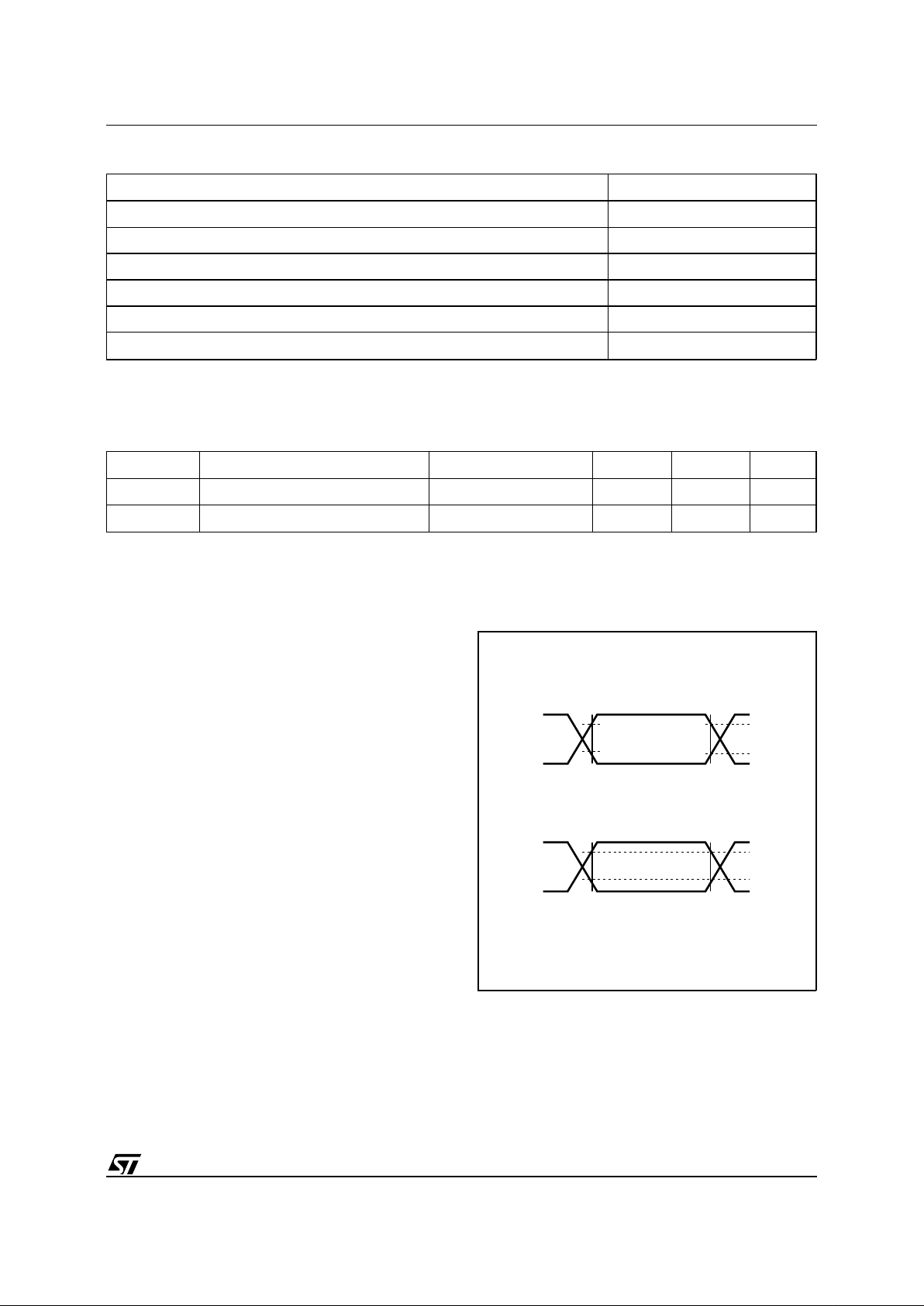
Input Rise and Fall Times
≤
50ns
Input Pulse Voltages (M93Sxx) 0.4V to 2.4V
Input Pulse Voltages (M93Sxx-W, M93Sxx-R) 0.2V
CC
to 0.8V
CC
Input Timing Reference Voltages (M93Sxx) 1.0V to 2.0V
Output Timing Reference Voltages (M93Sxx) 0.8V to 2.0V
Input and Output Timing Reference Voltages (M93Sxx-W, M93Sxx-R) 0.3V
CC
to 0.7V
CC
Output Load CL = 100pF
Note that Output Hi-Z is defined as the point where data is no longer driven.
T ab le 3. AC Measurement Conditions
AI02791
2.4V
0.4V
2.0V
0.8V
2V
1V
INPUT OUTPUT
0.8V
CC
0.2V
CC
0.7V
CC
0.3V
CC
M93SXX-W & M93SXX-R
M93SXX
Figure 3. AC Testing Input Output Waveforms
Symbol Parameter Test Condition Min Max Unit
C
IN
Input Capacitance VIN = 0V 5 pF
C
OUT
Output Capacitance V
OUT
= 0V 5 pF
Note:
1. Sampled only, not 100% tested.
T ab le 4. Capacitance
(1)
(T
A
= 25 °C, f = 1 MHz )
Within the time required by a programming cycle
(t
W
), up to 4 words may be written with help of the
Page Write instruction. the whole memory may also
be erased, or set to a predetermined pattern, by
using the Write All instruction.
Within the memory, an user defined area may be
protected against further Write instructions. The
size of this area is defined by the content of a
Protect Register, located outside of the memory
array. As a final prot ection s tep, data may be permanently protected by programming a One Time
Programming bit (OTP bit) which locks the Protect
Register content.
Programming is internally self-timed (the external
clock signal on C input may be disconnected or left
running after the start of a Write cycle) and does
not require an erase cycle prior to t he Write instruction. The Write instruction writes 16 bits at one time
into one of the 256/128/64 words of the
M93S46/S56/S66 respectively, the Page Write instruction writes up to 4 words of 16 bits to sequential locations, assuming in both cases that all
addresses are outside the Write Protected area.
After the start of the programming cycle, a
Ready/Busy signal is available on the Data output
(Q) when Chip Select (S) is driven High.
An internal feature of the M93Sx6 provides Poweron Data Protection by inhibiting any operation
when the Supply is too low. The design of the
M93Sx6 and the High Endurance CMOS technology used for its fabrication give an Erase/Write
cycle Endurance of 1,000,000 cycles and a data
retention of 40 years.
3/23
M93S66, M93S56, M93S46
Symbol Parameter Test Condition Min Max Unit
I
LI
Input Leakage Current 0V ≤ VIN ≤ V
CC
±
2.5
µ
A
I
LO
Output Leakage Current 0V ≤ V
OUT
≤ VCC, Q in Hi-Z
±
2.5
µ
A
I
CC
Supply Current VCC = 5V, S = VIH, f = 1 MHz 1.5 mA
I
CC1
Supply Current (Standby)
V
CC
= 5V, S = VSS, C = VSS,
W = V
SS
or VCC, PRE = VSS or VCC
50
µ
A
V
IL
Input Low Voltage
(D, C, S, W, PRE)
–0.3 0.8 V
V
IH
Input High Voltage
(D, C, S, W, PRE)
2V
CC
+ 1 V
V
OL
Output Low Voltage (Q) VCC = 5V, IOL = 2.1mA 0.4 V
V
OH
Output High Voltage (Q) VCC = 5V, IOH = –400µA 2.4 V
T ab le 5A. DC Characteristics for M93Sx6
(T
A
= 0 to 70°C or –40 to 85°C; VCC = 4.5V to 5.5V)
Symbol Parameter Test Condition Min Max Unit
I
LI
Input Leakage Current 0V ≤ VIN ≤ V
CC
±
2.5
µ
A
I
LO
Output Leakage Current 0V ≤ V
OUT
≤ VCC, Q in Hi-Z
±
2.5
µ
A
I
CC
Supply Current VCC = 5V, S = VIH, f = 1 MHz 1.5 mA
I
CC1
Supply Current (Standby)
V
CC
= 5V, S = VSS, C = VSS,
W = V
SS
or VCC, PRE = VSS or VCC
50
µ
A
V
IL
Input Low Voltage
(D, C, S, W, PRE)
–0.3 0.8 V
V
IH
Input High Voltage
(D, C, S, W, PRE)
2V
CC
+ 1 V
V
OL
Output Low Voltage (Q) VCC = 5V, IOL = 2.1mA 0.4 V
V
OH
Output High Voltage (Q) VCC = 5V, IOH = –400µA 2.4 V
T ab le 5B. DC Characteristics for M93Sx6
(T
A
= –40 to 125°C; VCC = 4.5V to 5.5V)
4/23
M93S66, M93S56, M93S46
Symbol Parameter Test Condition Min Max Unit
I
LI
Input Leakage Current 0V ≤ VIN ≤ V
CC
±
2.5
µ
A
I
LO
Output Leakage Current 0V ≤ V
OUT
≤ VCC, Q in Hi-Z
±
2.5
µ
A
I
CC
Supply Current (CMOS Inputs)
V
CC
= 5V, S = VIH, f = 1 MHz 1.5 mA
V
CC
= 2.5V, S = VIH, f = 1 MHz 1 mA
I
CC1
Supply Current (Standby)
V
CC
= 2.5V, S = VSS, C = VSS,
W = V
SS
or VCC, PRE = VSS or VCC
10
µ
A
V
IL
Input Low Voltage
(D, C, S, W, PRE)
–0.3 0.2 V
CC
V
V
IH
Input High Voltage
(D, C, S, W, PRE)
0.7 V
CC
VCC + 1 V
V
OL
Output Low Voltage (Q)
V
CC
= 5V, IOL = 2.1mA 0.4 V
V
CC
= 2.5V, IOL = 100µA 0.2 V
V
OH
Output High Voltage (Q)
V
CC
= 5V, IOH = –400µA 2.4 V
V
CC
= 2.5V, IOH = –100µAV
CC
– 0.2 V
T ab le 5C. DC Characteristics for M93Sx6-W
(T
A
= 0 to 70°C or –40 to 85°C; VCC = 2.5V to 5.5V)
Symbol Parameter Test Condition Min Max Unit
I
LI
Input Leakage Current 0V ≤ VIN ≤ V
CC
±
2.5
µ
A
I
LO
Output Leakage Current 0V ≤ V
OUT
≤ VCC, Q in Hi-Z
±
2.5
µ
A
I
CC
Supply Current (CMOS Inputs)
V
CC
= 3.6V, S = VIH, f = 1 MHz 1.5 mA
V
CC
= 1.8V, S = VIH, f = 1 MHz 1 mA
I
CC1
Supply Current (Standby)
V
CC
= 1.8V, S = VSS, C = VSS,
W = V
SS
or VCC, PRE = VSS or VCC
5
µ
A
V
IL
Input Low Voltage
(D, C, S, W, PRE)
–0.3 0.2 V
CC
V
V
IH
Input High Voltage
(D, C, S, W, PRE)
0.8 V
CC
VCC + 1 V
V
OL
Output Low Voltage (Q) VCC = 1.8V, IOL = 100µA 0.2 V
V
OH
Output High Voltage (Q) VCC = 1.8V, IOH = –100µAV
CC
– 0.2 V
Note:
1. This is preliminary data.
T ab le 5D. DC Characteristics for M93Sx6-R
(1)
(T
A
= 0 to 70°C or –20 to 85°C; VCC = 1.8V to3.6V)
5/23
M93S66, M93S56, M93S46
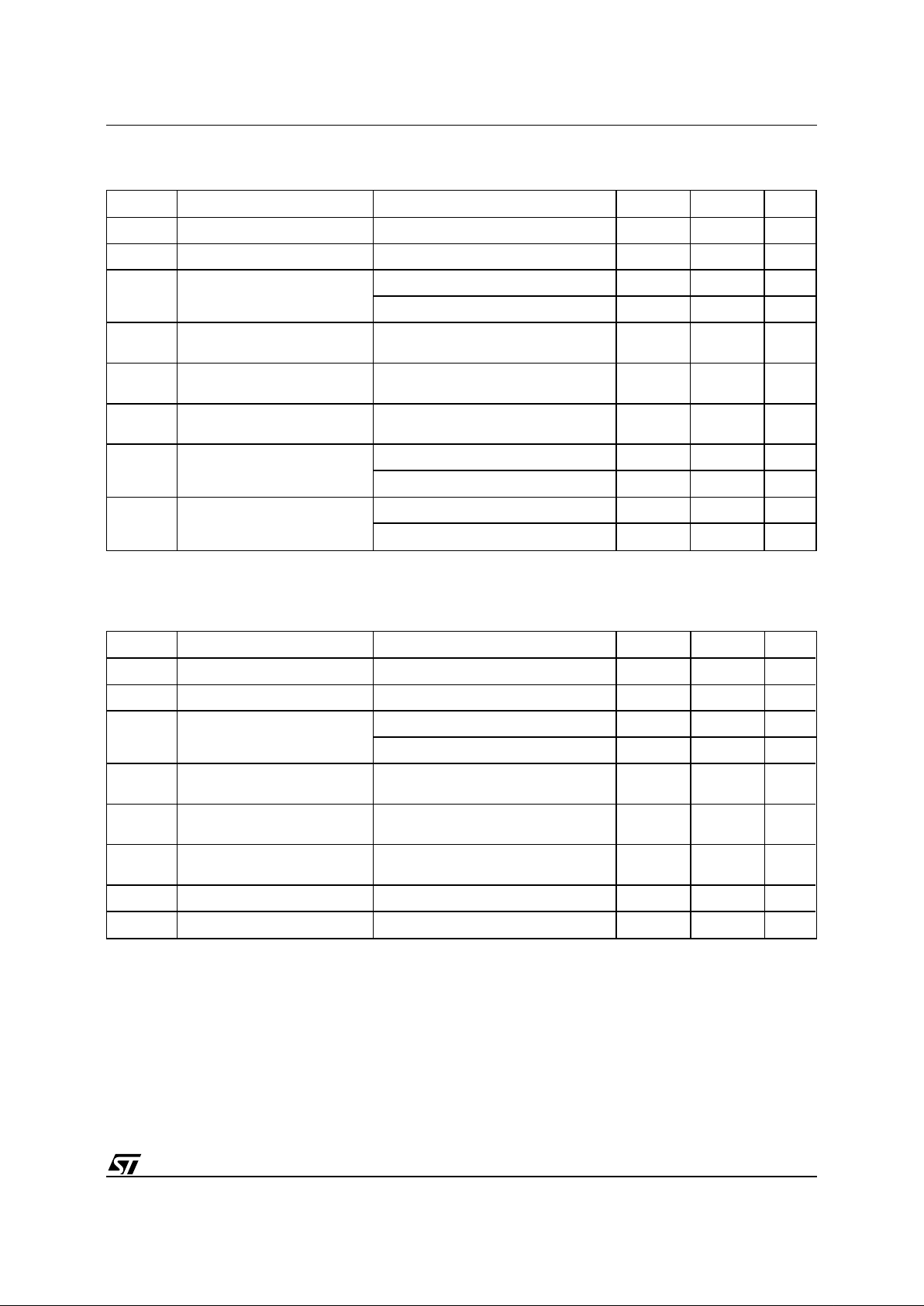
Symbol Alt Parameter
M93S66/56/46
Unit
V
CC
= 4.5V to 5.5V,
T
A
= 0 to 70°C,
T
A
= –40 to 85°C
V
CC
= 4.5V to 5.5V,
T
A
= –40 to 125°C
Min Max Min Max
t
PRVCH
t
PRES
Protect Enable Valid to Clock High 50 50 ns
t
WVCH
t
PES
Write Enable Valid to Clock High 50 50 ns
t
SHCH
t
CSS
Chip Select Set-up Time 50 50 ns
t
CLSH
t
SKS
Clock Set-up Time (relative to S) 100 100 ns
t
DVCH
t
DIS
Data In Set-up Time 100 100 ns
t
CHDX
t
DIH
Data In Hold Time 100 100 ns
t
CHQL
t
PD0
Delay to Output Low 400 400 ns
t
CHQV
t
PD1
Delay to Output Valid 400 400 ns
t
CLPRX
t
PREH
Clock Low to Protect Enable
Transition
00ns
t
SLWX
t
PEH
Chip Select Low to Write Enable
Transition
250 250 ns
t
CLSL
t
CSH
Chip Select Hold Time 0 0 ns
t
SLCH
Chip Select Low to Clock High 250 250 ns
t
SLSH
(1)
t
CS
Chip Select Low to Chip Select High 250 250 ns
t
SHQV
t
SV
Chip Select to Ready/Busy Status 400 400 ns
t
SLQZ
t
DF
Chip Select Low to Output Hi-Z 200 200 ns
t
CHCL
(2)
t
SKH
Clock High Time 250 250 ns
t
CLCH
(2)
t
SKL
Clock Low Time 250 250 ns
t
W
t
WP
Erase/Write Cycle time 10 10 ms
f
C
f
SK
Clock Frequency 0 1 0 1 MHz
Notes:
1. Chip Select must be brought low for a minimum of tSLSH between consecutive instructions cycles.
2. The Clock frequency specification calls for a minimum clock period of 1/fC, therefore the sum of the timings tCHCL+tCLCH
must be greater or equal to 1/fC.
T ab le 6A. AC Characteristics
6/23
M93S66, M93S56, M93S46
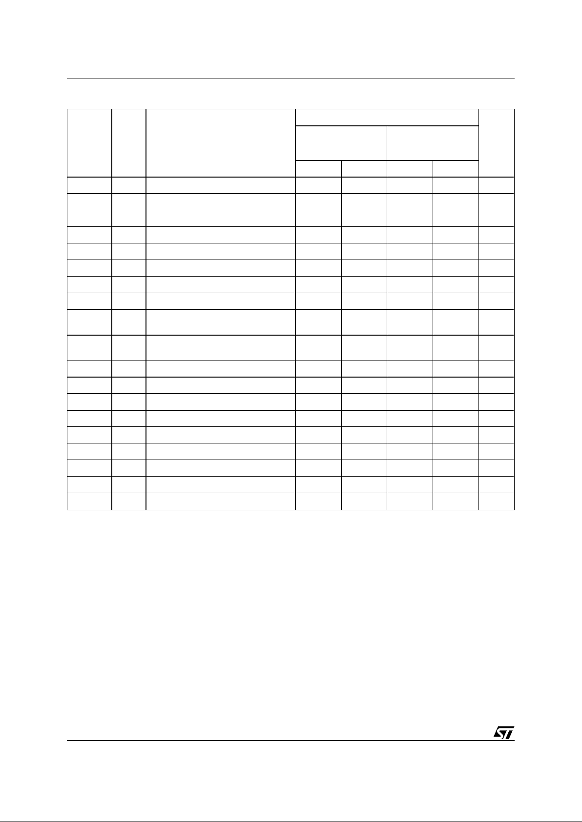
Symbol Alt Parameter
M93S66/56/46
Unit
V
CC
= 2.5V to 5.5V,
T
A
= 0 to 70°C,
T
A
= –40 to 85°C
V
CC
= 1.8V to 3.6V,
(3)
TA = 0 to 70°C
T
A
= –20 to 85°C
Min Max Min Max
t
PRVCH
t
PRES
Protect Enable Valid to Clock High 50 50 ns
t
WVCH
t
PES
Write Enable Valid to Clock High 50 50 ns
t
SHCH
t
CSS
Chip Select Set-up Time 100 200 ns
t
CLSH
t
SKS
Clock Set-up Time (relative to S) 100 100 ns
t
DVCH
t
DIS
Data In Set-up Time 100 100 ns
t
CHDX
t
DIH
Data In Hold Time 100 200 ns
t
CHQL
t
PD0
Delay to Output Low 400 700 ns
t
CHQV
t
PD1
Delay to Output Valid 400 700 ns
t
CLPRX
t
PREH
Clock Low to Protect Enable
Transition
00ns
t
SLWX
t
PEH
Chip Select Low to Write Enable
Transition
250 250 ns
t
CLSL
t
CSH
Chip Select Hold Time 0 0 ns
t
SLCH
Chip Select Low to Clock High 250 250 ns
t
SLSH
(1)
t
CS
Chip Select Low to Chip Select High 250 1000 ns
t
SHQV
t
SV
Chip Select to Ready/Busy Status 400 700 ns
t
SLQZ
t
DF
Chip Select Low to Output Hi-Z 200 200 ns
t
CHCL
(2)
t
SKH
Clock High Time 350 800 ns
t
CLCH
(2)
t
SKL
Clock Low Time 250 800 ns
t
W
t
WP
Erase/Write Cycle time 10 10 ms
f
C
f
SK
Clock Frequency 0 1 0 0.5 MHz
Notes:
1. Chip Select must be brought low for a minimum of tSLSH between consecutive instructions cycles.
2. The Clock frequency specification calls for a minimum clock period of 1/fC, therefore the sum of the timings tCHCL+tCLCH
must be greater or equal to 1/fC.
3. This is preliminary data.
T ab le 6B. AC Characteristics
7/23
M93S66, M93S56, M93S46

PRE
W
C
S
D
OP CODE OP CODESTART
START
OP CODE INPUT
tCHDXtDVCH
tCLSH tCLCH
tCHCLtWVCH
tPRVCH
AI02025
tSHCH
Figure 4. Synchronous Timing, Start and Op-Code Input
POWER-ON DATA PROTECTION
In order to prevent data corruption and inadvertent
write operations during power-up and power-down,
a Power On Reset (POR) circuit resets all internal
programming circuitry and sets the device in t he
Write Disable mode.
– At Power-up and Power-down, the device
must NOT be selected (that is, the S input
must be driven low) until the supply voltage
reaches the operating value Vcc specified in
the AC and DC tables.
– When V
CC
reaches its functional value, the device is properly reset (in the Write Disable
mode) and is ready to decode and execute an
incoming instruction.
For the M93Sx6 specified at 5V, the POR threshold
voltage is around 3V.
For all the other M93Sx6 specified at low V
CC
(with
-W and -R V
CC
range options), the POR threshold
voltage is around 1.5V.
8/23
M93S66, M93S56, M93S46

Figure 5. Synchronous Timing, Read or Write
AI002026
C
D
Q
ADDRESS INPUT
Hi-Z
tDVCH
tCLSL
A0
S
DATA OUTPUT
tCHQVtCHDX
tCHQL
An
tSLSH
tSLQZ
Q15 Q0
PRE
W
C
S
D
Hi-Z
tW
tDVCH
AI02027
Q
tCLPRX
tSLWX
tCLSL
tCHDX
tSLSH
tSLQZ
BUSY
tSHQV
READY
WRITE CYCLEADDRESS/DATA INPUT
An A0/D0
tSLCH
9/23
M93S66, M93S56, M93S46

INSTRUCTIONS
The M93S66/S56/S46 have eleven instructions, as
shown in Table 7. Each instruction is preceded by
the rising edge of the signal applied on the Chip
Select (S) input (assuming that the clock C is low).
After the device is selected, the internal logic waits
for the start bit, which define the begining of the
instruction bit stream. The start bit is the first ’1’ read
on D input during the rising edge of the clock C.
Following the start bit, the op-codes of the instructions are made up of the 2 following bits. Notice that
some instructions use only these first two bits,
others use also the first two bits of the address to
define the op-code. The op-code is then followed
by the address of the word to be accessed.
For the M93S46, the address is made up of 6 bits
(See Table 7a). For the M93S56 and M93S66, the
address is made up of 8 bit s (See Table 7b).
The M93Sx6 is fabricated in CMOS technology and
is therefore able to run from zero Hz (static input
signals) up to the maximum ratings (specified in
Table 6).
Instr. Description W PRE
Start
Bit
Op-
Code
Address
(1)
Data
Req.
Clock
Cycles
Additional
Information
READ
Read Data from
Memory
X ’0’ ’1’ 10 A5-A0 Q15-Q0
WRITE
Write Data to
Memory
’1’ ’0’ ’1’ 01 A5-A0 D15-D0 25
Write is executed
if the address is
not inside the
Protected area
PAWRITE
Page Write to
Memory
’1’ ’0’ ’1’ 11 A5-A0
N x
D15-D0
9 + N
x 16
Write is executed
if all the N
addresses are not
inside the
Protected area
WRALL
Write All
Memory
’1’ ’0’ ’1’ 00 01XXXX D15-D0 25
Write all data if
the Protect
Register is cleared
WEN Write Enable ’1’ ’0’ ’1’ 00 11XXXX 9
WDS Write Disable X ’0’ ’1’ 00 00XXXX 9
PRREAD
Protect
Register Read
X ’1’ ’1’ 10 XXXXXX
Q5-Q0
+ Flag
Data Output =
Protect Register
content + Protect
Flag bit
PRWRITE
Protect
Register Write
’1’ ’1’ ’1’ 01 A5-A0 9
Data above
specified address
A5-A0 are
protected
PRCLEAR
Protect
Register Clear
’1’ ’1’ ’1’ 11 111111 9
Protect Flag is
also cleared
(cleared Flag = 1)
PREN
Protect
Register
Enable
’1’ ’1’ ’1’ 00 11XXXX 9
PRDS
Protect
Register Disable
’1’ ’1’ ’1’ 00 000000 9
OTP bit is set
permanently
Note:
1. X = don’t care bit.
Table 7A. Instruction Set for the M93S46
10/23
M93S66, M93S56, M93S46

Instr. Description W PRE
Start
Bit
Op-
Code
Address
(1,2)
Data
Req.
Clock
Cycles
Additional
Information
READ
Read Data from
Memory
X ’0’ ’1’ 10 A7-A0 Q15-Q0
WRITE
Write Data to
Memory
’1’ ’0’ ’1’ 01 A7-A0 D15-D0 27
Write is executed
if the address is
not inside the
Protected area
PAWRITE
Page Write to
Memory
’1’ ’0’ ’1’ 11 A7-A0
N x
D15-D0
11 + N
x 16
Write is executed
if all the N
addresses are not
inside the
Protected area
WRALL
Write All
Memory
’1’ ’0’ ’1’ 00 01XXXXXX D15-D0 27
Write all data if
the Protect
Register is cleared
WEN Write Enable ’1’ ’0’ ’1’ 00 11XXXXXX 11
WDS Write Disable X ’0’ ’1’ 00 00XXXXXX 11
PRREAD
Protect
Register Read
X ’1’ ’1’ 10 XXXXXXXX
Q7-Q0
+ Flag
Data Output =
Protect Register
content + Protect
Flag bit
PRWRITE
Protect
Register Write
’1’ ’1’ ’1’ 01 A7-A0 11
Data above
specified address
A7-A0 are
protected
PRCLEAR
Protect
Register Clear
’1’ ’1’ ’1’ 11 11111111 11
Protect Flag is
also cleared
(cleared Flag = 1)
PREN
Protect
Register
Enable
’1’ ’1’ ’1’ 00 11XXXXXX 11
PRDS
Protect
Register Disable
’1’ ’1’ ’1’ 00 00000000 11
OTP bit is set
permanently
Notes:
1. X = don’t care bit.
2. Address bit A7 is not decoded by the M93S56.
T ab le 7B. Instruction Set for the M93S56 and M93S66
11/23
M93S66, M93S56, M93S46

Read
The Read instruction (READ) outputs serial data
on the Data Output (Q). When a READ instruction
is received, the instruction and address are decoded and the data from the memory is transferred
into an output shift register. A dumm y ’0’ bit is output
first followed by the 16 bit word with the MSB first.
Output data changes are trigger ed by the Low to
High transition of the Clock (C). T he M93Sx6 will
automatically increment the address and will clock
out the next word as long as the Chip Select input
(S) is held High. In this case the dummy ’0’ bit is
NOT output between words and a continuous
stream of data can be read.
Write Enable and Write Disable
The Write Enable instruction (WE N) authorizes the
following Write instructions to be executed. The
Write Disable instruction (WDS) disables the execution of the following Write instructions and the
internal programming cycle cannot run.
When power is first applied, the M93Sx6 is in Write
Disable mode and all Write inst ructions are inhibited. When the WEN instruction is executed, Write
instructions remain enabled until a Write Disable
instruction (WDS) is executed or V
CC
falls below
the Power-On Reset threshold Voltage.
To protect the memory contents from accidental
corruption, it is advisable to issue the WDS instruction after every write cycle. The READ instruction
is not affected by the WEN or WDS instructions.
Write
The Write instruction (WRITE) is composed of the
Start bit plus the Op-Code followed by the address
and the 16 data bits to be written. The Write E nable
signal (W) must be held high during the Write
instruction. Data input (D) is sampled on the Low
to High transition of the clock. After the last data bit
has been sampled, Chip Select (S) must be
brought Low before the next rising edge of the clock
(C) in order to start the self-timed programming
cycle. This is really important as, if S is brought low
before or after this specific frame window, the
addressed location will not be programmed, providing that the address in NOT in the protected area.
If the M93Sx6 is still performing the write cycle, the
Busy signal (Q = 0) will be returned if the Chip
Select input (S) is driven high after the t
SLSH
delay,
and the M93Sx6 will ignor e any data on t he bus.
When the write cycle is completed, the Ready
signal (Q = 1) will indicate (if S is driven high) that
the M93Sx6 is ready to receive a new instruction.
Programming is internally self-timed (the external
clock signal on C input may be disconnected or left
running after the start of a Write cycle).
Page Write
A Page Write instruction ( PAWRITE) contains the
first address to be written followed by up to 4 data
words. The Write Enable signal (W) must be held
High during the PAWRITE instruction. Input address and data are sampled on the Low to High
transition of the clock. After the receipt of each data
word, bits A1-A0 of the int ernal address register are
incremented, the high order bits (Ax-A2) remaining
unchanged. Users must take care by software to
ensure that the last wor d address has the same
upper order address bits as the initial address
transmitted to avoid address roll-over . After the LSB
of the last data word, Chip Select (S) must be
brought Low before the next rising edge of the
Clock (C) in order to start the self-timed programming cycle. This is really important as, if S is
brought low before or after this specific frame window, the addressed locations will not be programmed. The Page Write operation will not be
performed if any of t he 4 words is addr essing the
protected area. If the M93Sx6 is still performing the
programming cycle, the Busy signal (Q = 0) will be
returned if the Chip Select input (S) is driven high,
and the M93Sx6 will ignore any data on the bus.
When the write cycle is completed, the Ready
signal (Q = 1) will indicate (if S is driven high) that
the M93Sx6 is ready to rec eiv e a new instruction.
Write All
The Write All instruction (W RALL) is valid only af ter
the Protect Register has been cleared by executing
a PRCLEAR (Protect Register Clear) instruction.
The Write All instruction simultaneously writes the
whole memory with the same data word included
in the instruction. The Write Enable signal (W) must
be held High before and during t he Write All instruction. Input address and dat a are sampled on the
Low to High transition of the clock. If the M93Sx6
is still performing the write cycle, the Busy signal
(Q = 0) will be returned if the Chip Select input (S)
is driven high after the t
SLSH
delay, and the M93Sx6
will ignore any data on the bus. When the write
cycle is completed, the Ready signal (Q = 1) will
indicate (if S is driven high) that the M93Sx6 is
ready to receive a new instruction.
READY/BUSY Status
During every programming cycle (after a WRITE,
WRALL or PAWRITE instruction) the Data Output
(Q) indicates the Ready/Busy status of the memory
when the Chip Select is driven High. Once the
M93Sx6 is Ready , the Data Output is s et to ’1’ until
a new start bit is decoded or the Chip Select is
brought Low.
12/23
M93S66, M93S56, M93S46

MEMORY WRITE PROTECTION AND PROTECT
REGISTER
The M93Sx6 offers a Protect Register containing
the bottom address of the memory area which has
to be protected against write instructions. In addition to this Protect Register, two flag bits are used
to indicate the Protect Register status: the Protect
Flag enabling/disabling the memory protection
throught the Protect Register and the OTP bit
which, when set, disables access to the Protect
Register and thus prevents any further modifications of this Protect Register value. The content of
the Protect Register is defined when using the
PRWRITE instruction, it may be read when usi ng
the PRREAD instruction. A specific instruction
PREN (Protect Register Enable) allows the user to
execute the protect instructions PRCLEAR,
PRWRITE and PR DS. this PREN instruc tion being
used together with the signals applied on the input
pins PRE (Protect Register Enable) and W (Write
Enable).
Accessing the Protect Register is done by executing the following sequence:
– WEN: execute the Write Enable instruction,
– PREN: execute the PREN instruction,
– PRWRITE, PRCLEAR or PRDS: the protection
then may be defined, in terms of size of the
protected area (PRWRITE, PRCLEAR) and
may be set permanently (PRDS instruction).
Protect Register Read
The Protect Register Read instruction (PRREAD)
outputs on the Data Output Q the content of the
Protect Register, followed by the Protect Flag bit.
The Protect Register Enable pin (PRE) must be
driven High before and during the instruction.
As in the Read instruction a dummy ’0’ bit is output
first. Since it is not possible to distinguish if the
Protect Register is cleared (all 1’s) or if it is written
with all 1’s, user must c heck the Protect Flag status
(and not the Protect Register content) to ascertain
the setting of the memory protection.
Protect Register Enable
The Protect Register Enable instruction (PREN) is
used to authorize the use of further PRCLEAR,
PRWRITE and PRDS instructions. The PREN
insruction does not modify the Protect Flag bit
value.
Note: A Write Enable (WEN) instruction must be
executed before the Protect Enable instruction.
Both the Protect Enable (PRE) and Write Enab le
(W) input pins must be held High during the instruction execution.
Protect Register Clear
The Protect Register Clear instruction (PRCLEAR)
clears the address s tored in the Protect Register to
all 1’s, and thus enables the execution of WRITE
and WRALL instructions. The Protect Register
Clear execution clears the Protect Flag to ’1’. Both
the Protect Enable (PRE) and Write Enable (W)
input pins must be driven High during the instruction execution.
Note: A PREN instruction must immediately precede the PRCLEAR instruction.
Protect Register Write
The Protect Register Write instruction (PRWRITE)
is used to write into the Protect Register the address of the first word to be protected. After the
PRWRITE instruction execution, all memory locations equal to and above the s pecified address, are
protected from writing. The Protect Flag bit is set to
’0’, it can be read with Protect Register Read
instruction. Both the Protect Enable (PRE) and
Write Enable (W) input pins must be driven High
during the instruction execution.
Note: A PREN instruction must immediately precede the PRWRITE instruction, but it is not necessary to execute first a PRCLEAR.
Protect Register Disable
The Protect Register Disable instruction sets the
One Time P rogrammable bit (OTP bit). The Protect
Register Disable instruction (PRDS) is a ONE TIME
ONLY instruction which latches the Protect Register content, this content is therefore unalterable in
the future. Both the Protect Enable (PRE) and Write
Enable (W) input pins must be driven High during
the instruction execution. The OTP bit cannot be
directly read, it can be checked by reading the
content of the Protect Register (PRREAD instruction), then by writing this same value into the Protect Register (PRWRITE instruction): when the
OTP bit is set, the Ready/Busy status cannot appear on the Data output (Q). When the OTP bit is
not set, the Busy status appear on the Data output
(Q).
Note: A PREN instruction must immediately precede the PRDS instruction.
13/23
M93S66, M93S56, M93S46

AI00889D
1 1 0 An A0
Qn Q0
DATA OUT
D
S
Q
S
WRITE
ADDR
OP
CODE
1 0An A0
DATA IN
D
Q
OP
CODE
Dn D01
BUSY READY
S
WRITE
ENABLE
1 0XnX0D
OP
CODE
101
S
WRITE
DISABLE
1 0XnX0D
OP
CODE
0 00
CHECK
STATUS
ADDR
PREREAD
PRE
W
PRE
W
PRE
Figure 6. READ, WRITE, WEN, WDS Sequences
Notes:
1. An - Xn - Qn - Dn: Refer to T able 7a for the M93S46.
2. An - Xn - Qn - Dn: Refer to Table 7b for the M93S56 and M93S66.
14/23
M93S66, M93S56, M93S46

AI00890C
S
PAGE
WRITE
1 1An A0
DATA IN
D
Q
OP
CODE
Dn D01
BUSY READY
CHECK
STATUS
ADDR
PRE
W
S
WRITE
ALL
1 0XnX0
DATA IN
D
Q
OP
CODE
Dn D00
BUSY READY
CHECK
STATUS
ADDR
PRE
W
01
Figure 7. PAWRITE, WRALL Sequences
Notes:
1. An - Xn - Dn: Refer to Table 7a for the M93S46.
2. An - Xn - Dn: Refer to Table 7b for the M93S56 and M93S66.
15/23
M93S66, M93S56, M93S46

Notes:
1. An - Xn - Dn: Refer to Table 7a for the M93S46.
2. An - Xn - Dn: Refer to Table 7b for the M93S56 and M93S66.
AI00891D
1 1 0 Xn X0
DATA
OUT
D
S
Q
S
Protect
Register
WRITE
ADDR
OP
CODE
1 0An A0D
Q
OP
CODE
1
BUSY READY
S
Protect
Register
ENABLE
1 0XnX0D
OP
CODE
101
CHECK
STATUS
ADDR
PREProtect
Register
READ
PRE
W
PRE
W
An A0 F
F = Protect Flag
Figure 8. PRREAD, PRWRITE, PREN Sequences
16/23
M93S66, M93S56, M93S46

Notes:
1. An - Xn - Dn: Refer to Table 7a for the M93S46.
2. An - Xn - Dn: Refer to Table 7b for the M93S56 and M93S66.
AI00892C
S
Protect
Register
CLEAR
1 1D
Q
OP
CODE
1
BUSY READY
CHECK
STATUS
ADDR
PRE
W
111
S
Protect
Register
DISABLE
1 0D
Q
OP
CODE
0
BUSY READY
CHECK
STATUS
ADDR
PRE
W
000
Figure 9. PRCLEAR, PRDS Sequences
17/23
M93S66, M93S56, M93S46

AI01395
S
An-1
C
D
WRITE
START
D0"1""0"
An
Glitch
An-2
ADDRESS AND DATA
ARE SHIFTED BY ONE BIT
Figure 10. Write Sequence with One Clock Glitch
COMMON I/O OPERA TION
The Data Output (Q) and Data Input ( D) signals can
be connected together, through a current limiting
resistor, to form a common, one wire data bus.
Some precautions must be taken when oper ating
the memory with this connection, mostly to prevent
a short circuit between the last entered address bit
(A0) and the first data bit output by Q. The reader
should refer to the STMicroelectronics application
note AN394 "MICROWIRE EEPROM Common I/O
Operation".
CLOCK PULSE COUNTER
The M93Sx6 offers a functional security filtering
glitches on the clock input (C), the clock pulse
counter.
In a normal environment, the M93Sx6 expectes to
receive the exact amount of data on the D input
(start bit, Op-Code, Address, Data), that is the
exact amount of clock pulses on t he C input. In a
noisy environment, the number of pulses received
(on the clock input C) may be greater than the clock
pulses delivered by the Master (Microcontroller)
driving the M93Sx6. In such a case, a part of the
instruction is delayed by one bit (see Figure 10),
and it may induce an erroneous write of data at a
wrong address. The M93Sx6 has an on-chip
counter which counts the clock pulses from the
Start bit until the falling edge of the Chip Select
signal.
For the WRITE instructions with a M93S56 (or
M93S66), the number of clock pulses incoming to
the counter must be exactly 27 from the Start bit to
the falling edge of Chip Select signal (1 Start bit +
2 Op-code bit + 8 Address bit + 16 Data bit = 27):
if so, the M93S56 (or M93S66) executes the
WRITE instruction. If the number of clock pulses is
not equal to 27, the instruction will not be ex ecuted
(and data will not be corrupted).
The clock pulse counter is active on WRITE,
PAWRITE, WRALL, PRWRITE and PRCLEAR instructions. In order to determine the exact number
of clock pulses needed for all the M93Sx6 on
WRITE instructions, refer to Tables 7a and 7b, in
the column: Requested Clock Cycles.
18/23
M93S66, M93S56, M93S46

ORDERING INFORMATION SCHEME
Devices are shipped from the factory with the memory content set at all "1’s" (FFFFh).
For a list of available options (Operating Voltage, Package, etc...) or for further information on any aspect
of this device, please contact the STMicroelectronics Sales Office nearest to you.
Memory Density
66 4 Kbit
56 2 Kbit
46 1 Kbit
Operating Voltage
blank4.5V to 5.5V
W 2.5V to 5.5V
R
(3)
1.8V to 3.6V
Package
BN PSDIP8
0.25mm Frame
MN SO8
150mil Width
DW TSSOP8
169mil Width
Temperature Range
1
(1)
0 to 70 °C
5 –20 to 85 °C
6 –40 to 85 °C
3
(2)
–40 to 125 °C
Option
T Tape & Reel
Packing
Example: M93S56 – W MN 6 T
Notes:
1. Temperature range on request only.
2. Produced with High Reliability Certified Flow (HRCF), in V
CC
range 4.5V to 5.5V at 1MHz only.
3. -R version (1.8V to 3.6V) are only available in temperature ranges 5 or 1.
19/23
M93S66, M93S56, M93S46

PSDIP-a
A2
A1AL
e1
D
E1 E
N
1
C
eA
eB
B1
B
Symb
mm inches
Typ Min Max Typ Min Max
A 3.90 5.90 0.154 0.232
A1 0.49 – 0.019 –
A2 3.30 5.30 0.130 0.209
B 0.36 0.56 0.014 0.022
B1 1.15 1.65 0.045 0.065
C 0.20 0.36 0.008 0.014
D 9.20 9.90 0.362 0.390
E 7.62 – – 0.300 – –
E1 6.00 6.70 0.236 0.264
e1 2.54 – – 0.100 – –
eA 7.80 – 0.307 –
eB 10.00 0.394
L 3.00 3.80 0.118 0.150
N8 8
Drawing is not to scale
PSDIP8 - 8 pin Plastic Skinny DIP, 0.25mm l ead frame
20/23
M93S66, M93S56, M93S46

SO-a
E
N
CP
B
e
A
D
C
LA1 α
1
H
h x 45˚
Symb
mm inches
Typ Min Max Typ Min Max
A 1.35 1.75 0.053 0.069
A1 0.10 0.25 0.004 0.010
B 0.33 0.51 0.013 0.020
C 0.19 0.25 0.007 0.010
D 4.80 5.00 0.189 0.197
E 3.80 4.00 0.150 0.157
e1.27– –0.050– –
H 5.80 6.20 0.228 0.244
h 0.25 0.50 0.010 0.020
L 0.40 0.90 0.016 0.035
α
0
°
8
°
0
°
8
°
N8 8
CP 0.10 0.004
Drawing is not to scale
SO8 - 8 lead Plastic Small Outline, 150 mils body width
21/23
M93S66, M93S56, M93S46

TSSOP
1
N
CP
N/2
DIE
C
L
A1
EE1
D
A2A
α
eB
Symb
mm inches
Typ Min Max Typ Min Max
A 1.10 0.043
A1 0.05 0.15 0.002 0.006
A2 0.85 0.95 0.033 0.037
B 0.19 0.30 0.007 0.012
C 0.09 0.20 0.004 0.008
D 2.90 3.10 0.114 0.122
E 6.25 6.50 0.246 0.256
E1 4.30 4.50 0.169 0.177
e0.65– –0.026– –
L 0.50 0.70 0.020 0.028
α
0
°
8
°
0
°
8
°
N8 8
CP 0.08 0.003
Drawing is not to scale
TSSOP8 - 8 lead Plastic Shrink Small Outline, 169 mils body width
22/23
M93S66, M93S56, M93S46

Information furnished is believ ed to be accurate and reliable. However, STMicroelectronics assumes no responsi bility for the consequences
of use of such information nor for any infringement of patents or other rights of third parties which may result from its use. No license is granted
by implication or otherwise under any patent or patent rights of STMicroelectronics. Specifications mentioned in this publication are subject to
change without notice. This publication supersedes and repl aces all information previously supplied. STMicroelectron ics products are not
authorized for use as critical components in life support devices or systems without express written approval of STMicroelectronics.
The ST logo is a registered trademark of STMicroelect roni cs
© 1999 STMicroelectronics - All Rights Reserved
All other names are the property of their respective owners
STMicroelectronics GROUP OF COMPANIES
Australia - Brazil - Canada - China - France - Germany - Italy - Japan - Korea - Malaysia - Malta - Mexico - Morocco - The Netherlands -
Singapore - Spain - Sweden - Switzerland - T aiwan - Thailand - United Kingdom - U.S.A.
http://www.st.com
23/23
M93S66, M93S56, M93S46
 Loading...