

SGS Thomson Microelectronics M8934F2W, M8913F2Y, M8913F2W, M8913F1Y, M8913F1W Datasheet
...
M89 FAMILY
In-System Programmable (ISP)
Multiple-Memory and Logic FLASH+PSD Systems for MCUs
DATA BRIEFING
■ Single Supply Voltage:
–5V±10% for M89xxFxY
– 3 V (+20/–10%) for M89xxFxW
■ 1 or2 Mbit of Primary Flash Memory (8 uniform
sectors, 16K x 8, or 32K x 8)
■ A second non-volatile memory:
– 256 Kbit (32K x 8) EEPROM (for M8913F1x)
or Flash memory (for M89x3F2x)
– 4 uniform sectors (8K x 8)
■ SRAM (16 Kbit, 2K x 8; or 64 Kbit, 8K x 8)
■ Over 2,000 Gates of PLD: DPLD and GPLD
■ 27 Reconfigurable I/O ports
■ Enhanced JTAG Serial Port
■ Programmable power management
■ Stand-by current:
–50µA for M89xxFxY
–25µA for M89xxFxW
■ High Endurance:
– 100,000 Erase/Write Cycles of Flash Memory
– 10,000 Erase/Write Cycles of EEPROM
– 1,000 Erase/Write Cycles of PLD
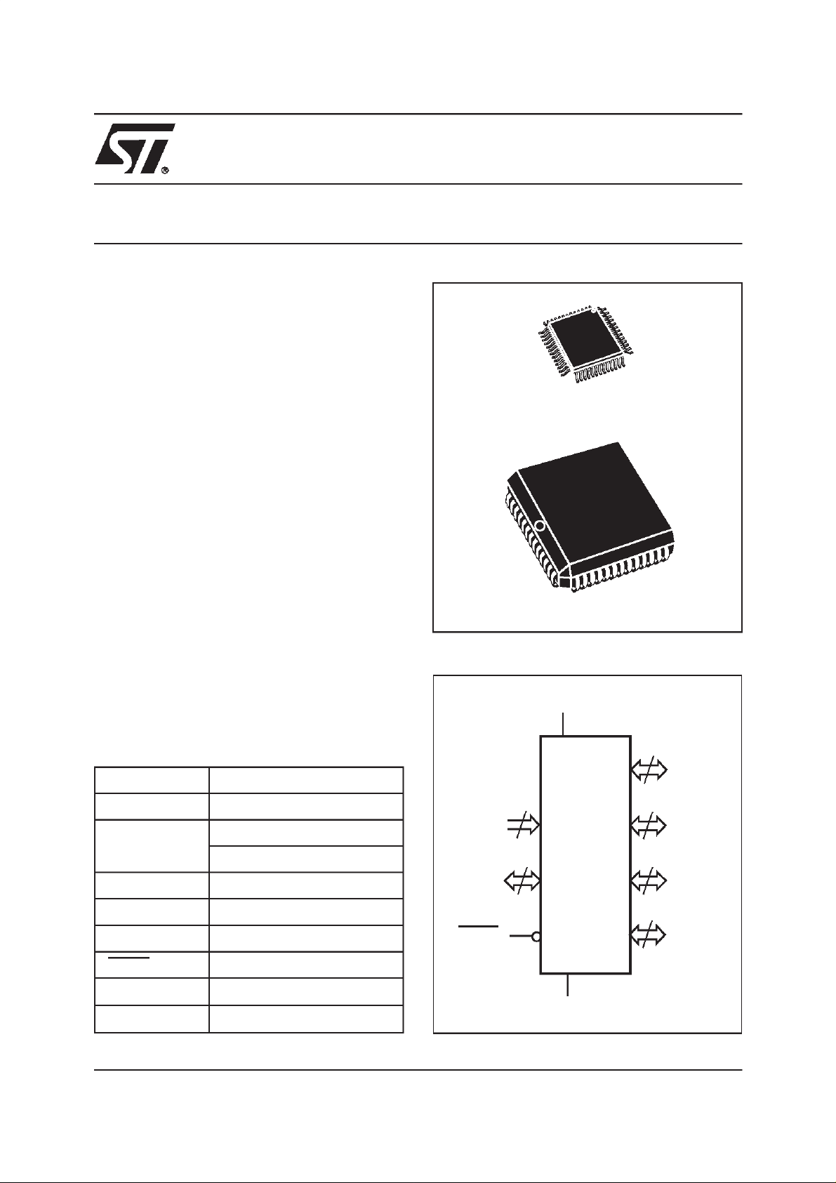
Figure 1. Logic Diagram
PQFP52 (T)
PLCC52 (K)
Table 1. Signal Names
PA0-PA7 Port-A
PB0-PB7 Port-B
PC0-PC7
PD0-PD2 Port-D
AD0-AD15 Address/Data
CNTL0-CNTL2 Control
RESET Reset
V
CC
V
SS
June 2000
Complete data available on
Port-C
PC2 = Voltage Stand-by
Supply Voltage
Ground
Data-on-Disc CD-ROM
or at
www.st.com
V
CC
8
PA0-PA7
3
CNTL0-
8
PB0-PB7
CNTL2
FLASH+PSD
16
8
AD0-AD15 PC0-PC7
3
RESET
V
SS
PD0-PD2
AI02856
1/7

M89 FAMILY
Figure 2A. PLCC Connections
RESET
PB7
CNTL1
CNTL2
CNTL0
47
48
49
50
51
AD15
46
AD14
45
AD13
44
AD12
43
AD11
42
AD10
41
AD9
40
AD8
39
VCC
38
AD7
37
AD6
36
AD5
35
AD4
34
PA0
AD1
AD2
AD3
AD0
AI02857
VCC
GND
PD2
PD1
PD0
PC7
PC6
PC5
PC4
PC3
PC2
PC1
PC0
PB0
PB1
PB2
PB3
PB4
PB5
GND
PB6
52
2
34567
PA4
PA3
GND
1
PA2
PA1
8
9
10
11
12
13
14
15
16
17
18
19
20
21222324252627282930313233
PA7
PA6
PA5
DESCRIPTION
The FLASH+PSD family of memory systems for
microcontrollers (MCUs) brings In-SystemProgrammability (ISP) to Flash memory and
programmable logic. The result is a simple and
flexible solution for embedded designs.
FLASH+PSD devices combine many of the
peripheral functions found in MCU based
applications. FLASH+PSD provides a glueless
interface to most commonly-used ROMless
MCUs.
Table 2 summarizes all the devices in the M89
Family.
The FLASH+PSD device includes a JTAG Serial
Programming interface, to allow In-System
Programming (ISP) of the entire device. This
Figure 2B. PQFP Connections
PB0
PB1
PB2
PB3
PB4
PB5
GND
PB6
PB7
CNTL1
CNTL2
RESET
44
22
PA0
43
23
AD0
42
24
AD1
41
25
AD2
CNTLO
40
26
AD3
39
38
37
36
35
34
33
32
31 VCC
30
29
28
27 AD4
AD15
AD14
AD13
AD12
AD11
AD10
AD9
AD8
AD7
AD6
AD5
AI02858
PD2
PD1
PD0
PC7
PC6
PC5
PC4
VCC
GND
PC3
PC2
PC1
PC0
52
51
50
49
48
47
46
45
1
2
3
4
5
6
7
8
9
10
11
12
13
14
15
16
17
18
19
20
21
PA7
PA6
PA5
PA4
PA3
PA2
PA1
GND
feature reduces development time, simplifies the
manufacturing flow, and dramatically lowers the
cost of field upgrades. Using ST’s special FastJTAG programming, a design can be rapidly
programmed into the FLASH+PSD.
The innovative FLASH+PSD family solves key
problems faced by designers when managing
discrete Flash memory devices, such as:
– Complex address decoding
– In-System (first-time) Programming (ISP)
– Concurrent EEPROM or Flash memory
programming (IAP).
The JTAG Serial Interface block allows In-System
Programming (ISP). Embedded dual-bank
memories eliminates the need for an external Boot
Table 2. Product Range
Part Number
Primary Flash
1
Memory
Secondary NVM
SRAM
2
I/O Ports Voltage Range Access Time
M8913F1Y 1 Mbit 256 Kbit EEPROM 16 Kbit 27
M8913F2Y 1 Mbit 256 Kbit Flash memory 16 Kbit 27
4.5-5.5 V
90 ns or
150 ns
M8934F2Y 2 Mbit 256 Kbit Flash memory 64 Kbit 27
M8913F1W 1 Mbit 256 Kbit EEPROM 16 Kbit 27
2.7-3.6 V 150 nsM8913F2W 1 Mbit 256 Kbit Flash memory 16 Kbit 27
M8934F2W 2 Mbit 256 Kbit Flash memory 64 Kbit 27
Note: 1. All products support: JTAG serial ISP, MCU parallel ISP, ISP Flash memory, ISP GPLD, Security features, Power Management
Unit (PMU), Automatic Power-down (APD)
2. SRAM may be backed up using an external battery.
2/7
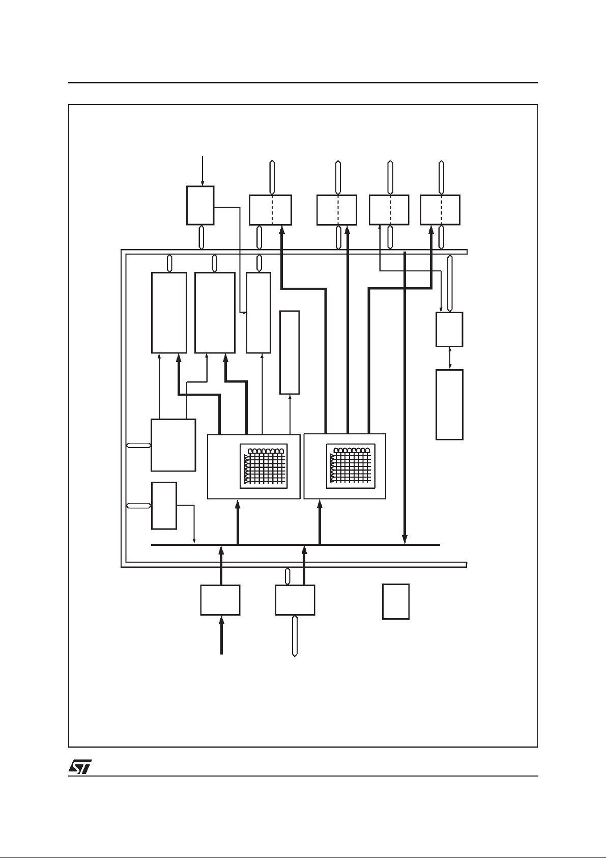
Figure 3. FLASH+PSD Block Diagram
)
PC2
(
VSTDBY
PA0 – PA7
PB0 – PB7
PC0 –PC7
M89 FAMILY
PD0 –PD2
ADDRESS/DATA/CONTROL BUS
MEMORY
1 OR 2 MBITMAIN FLASH
8 SECTORS
EMBEDDED
ALGORITHM
UNIT
POWER
MANGMT
256 KBITSECONDARY
SECTOR
4 SECTORS
FLASH MEMORY
(BOOT OR DATA)
SELECTS
)
DPLD
(
PLD
FLASH DECODE
SECTOR
SELECTS
PORT
PROG.
BACKUP SRAM
16 OR 64 KBIT BATTERY
SRAM SELECT
A
PORT
RUNTIME CONTROL
CSIOP
AND I/O REGISTERS
FLASH ISP PLD
PORT
PROG.
GPLD OUTPUT
(GPLD)
B
PORT
GPLD OUTPUT
PROG.
GPLD OUTPUT
PORT
C
PORT
I/O PORTPLD INPUT
PORT
PORT
PROG.
JTAG
SERIAL
PLD, CONFIGURATION
D
CHANNEL
LOADER
& FLASHMEMORY
PAGE
PLD
BUS
INPUT
REGISTER
PROG.
CNTL0,
CNTL1,
MCU BUS
CNTL2
57
INTRF.
ADIO
AD0 – AD15
PORT
57
GLOBAL
CONFIG. &
SECURITY
AI03765
Sometimes computers try to be too clever for theirown good. Take this illustration for instance.
Just because somany of the labels are rotatedthrough ninety degrees, FrameMaker seems to
want to insist on telling the postscript file that I would find it more convenient to see this page
displayed inlandscape, rotated by ninety degrees. Well I wouldn’t. So I amputting inall this text
just to weight the average in this direction.
3/7
 Loading...