

SGS Thomson Microelectronics M87C257 Datasheet

256K (32K x 8) UV EPROM and OTP EPROM
INTEGRA TE D ADDRE SS LATCH
FA ST ACCESS TIME: 45ns
LOW POWER “CMOS” CONSUMPTION:
– Active Current 30mA
– Standby Current 100µA
PROGRAMMING VOLTAGE: 12.75V
ELECTRONI C S IG NATURE for AUTOM ATED
PROGRAMMING
PROGRAM MING T IM ES of ARO UND 3sec.
(PRESTO II ALGORITHM)
DESCRIP TION
The M87C257 is a high speed 262,144 bit UV
erasable and electrically programmable EPROM.
The M87C257 incorporates latches for all address
inputs to minimize chip count, reduce cost, and
simplify the design of multiplexed bus systems.
The Window Ceramic Frit-Seal Dual-in-Line package has a transparent lid which allows the user to
expose the chip to ultraviolet light to erase the bit
pattern. A new pattern can then be written to the
device by following the programming procedure.
For applications where the content is pr ogrammed
only one time and erasure is not required, the
M87C257 is offered in Plas tic Leaded Chip Carrier ,
package.
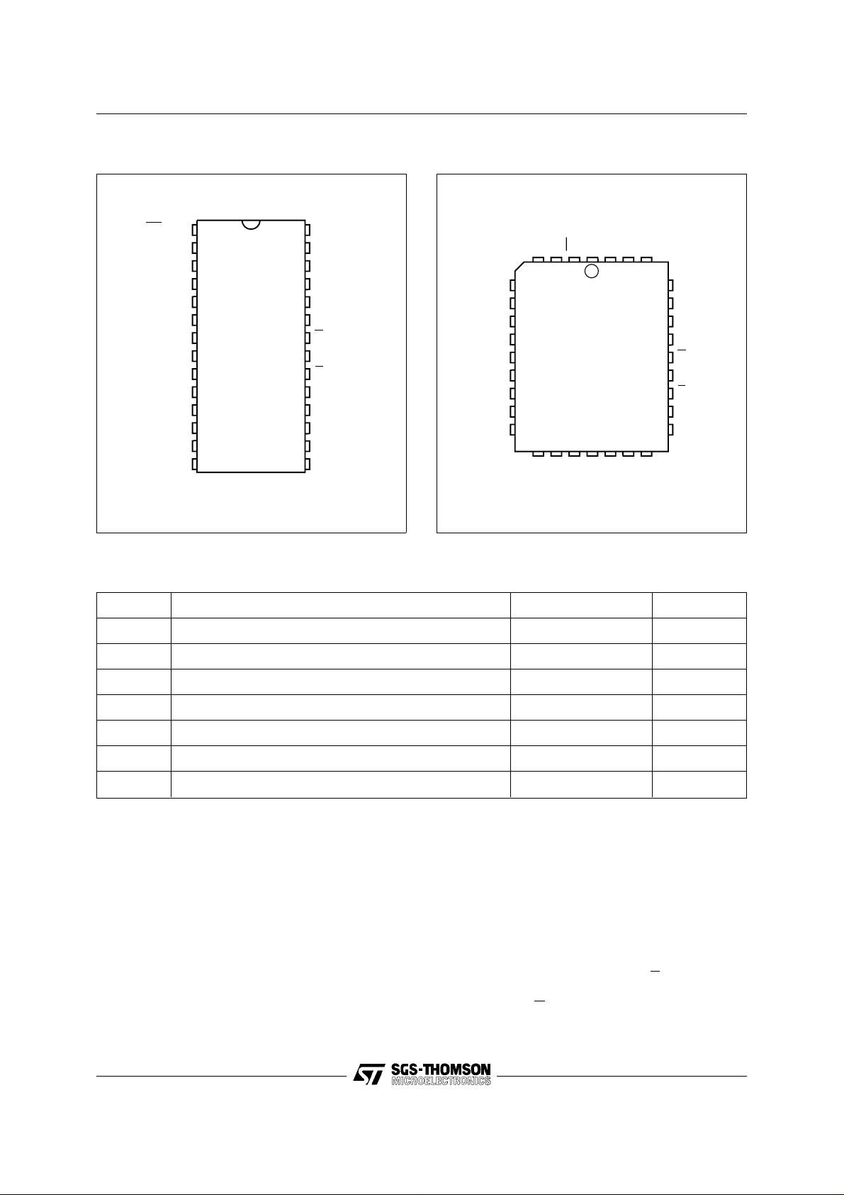
ADDRESS LATCHED
28
1
FDIP28W (F)
Figure 1. Logic Diag ra m
V
CC
15
A0-A14
E
M87C257
M87C257
PLCC32 (C)
8
Q0-Q7
G
T able 1. Signal Names
A0 - A14 Address Inputs
Q0 - Q7 Data Outputs
E Chip Enable
G Output Enable
ASV
PP
V
CC
V
SS
June 1996 1/13
Address Strobe / Program Supply
Supply Voltage
Ground
ASV
PP
V
SS
AI00928B
M87C257
Figure 2A. DIP Pin Connecti on s
ASV
PP
A12
A7
A6
A5
A4
A3
A2
A1
A0
Q0
Q2
SS
1
2
3
4
5
6
7
8
9
10
11
12
13
14
M87C257
28
27
26
25
24
23
22
21
20
19
18
17
16
15
AI00929
V
CC
A14
A13
A8
A9
A11
G
A10
E
Q7
Q6
Q5Q1
Q4
Q3V
Figure 2B. LCC Pin Conn ecti ons
PP
CC
A13
DU
32
DU
V
Q3
A14
Q4
25
Q5
A8
A9
A11
NC
G
A10
E
Q7
Q6
AI00930
ASV
A7
A12
1
A6
A5
A4
A3
A2
9
M87C257
A1
A0
NC
Q0
17
Q1
Q2
SS
V
Warning: NC = Not Connected, DU = Dont’t Use.
Tab l e 2. Absolu te Maxi mu m Ratin gs
Symbol Parameter Value Unit
T
A
T
BIAS
T
STG
(2)
V
IO
V
CC
(2)
V
A9
V
PP
Notes: 1. Except for the rating "Operating Temperature Range", stresses above those lis ted in the Table "Absolute Maximum Ratings"
2. Minimum DC voltage on Input or Output is –0.5V with possible undershoot to –2.0V for a period less than 20 ns. Maximum DC
Ambient Operating Temperature –40 to 125 °C
Temperature Under Bias –50 to 125 °C
Storage Temperature –65 to 150 °C
Input or Output Voltages (except A9) –2 to 7 V
Supply Voltage –2 to 7 V
A9 Voltage –2 to 13.5 V
Program Supply Voltage –2 to 14 V
may cause permanent damage to the device. These are stress ratings only and operation of the device at these or any other
conditions above those indicated in the Operating sections of this specificat ion is not implied. Exposure to Abs olute Maxi mum
Rating conditions for extended periods may affect device reliability . Refer also to the SGS-THOMS O N SURE Program and other
relevant quality documents.
voltage on Output is V
+0.5V with possible ove rshoot to VCC +2V for a period less than 20ns.
CC
DEVICE OPER ATION
The modes of operation of the M87C257 are listed
in the Operating Modes. A single power supply is
required in the read mode. All inputs are T TL levels
except for V
and 12V on A9 for Elect ronic S igna-
PP
ture.
(1)
Read Mode
The M87C257 has two control functions, both of
which must be logically active in order to obtain
data at the outputs. Chip Enable (
E) is the power
control and should be used for device selection.
Output Enable (
G) is the output control and should
2/13
T ab le 3. Operating Modes
M87C257
Mode E GA9ASV
Read (Latched Address) V
Read (Applied Address) V
Output Disable V
Program V
Verify V
Program Inhibit V
Standby V
Electronic Signature V
Note: X = VIH or VIL, VID = 12V ± 0.5V
IL
IL
IL
Pulse V
IL
IH
IH
IH
IL
V
IL
V
IL
V
IH
IH
V
IL
V
IH
X X X Hi-Z
V
IL
XVILData Out
XVIHData Out
X X Hi-Z
XVPPData In
XVPPData Out
XVPPHi-Z
V
ID
PP
V
IL
T ab le 4. Electron ic Sig natu r e
Identifier A0 Q7 Q6 Q5 Q4 Q3 Q2 Q1 Q0 Hex Data
Manufacturer’s Code V
Device Code V
IL
IH
be used to gate data to the output pins, independent of device selection. Assuming that the
addresses are stable (
), the address access time (t
V
IL
delay from
E to output (t
the output after delay of t
G, assuming that E has been low and the ad-
of
AS = VIH) or latched (AS =
ELQV
GLQV
dresses have been stable for at least t
The M87C257 reduces the hardware interface in
multiplexed address-data bus systems. The processor multiplexed bus (AD0-AD7) may be tied to
the M87C257’s address and data pins. No separate address latch is needed because the
M87C257 latches all address inputs when
low.
Standby Mode
The M87C257 has a standby mode which reduces
the active current from 30mA to 100µA (Address
Stable). The M87C257 is placed in the standby
mode by applying a CMOS high signal to the
00100000 20h
10000000 80h
Two Line Output Control
Because EPROMs are usually used in larger mem-
) is equal to the
AVQV
). Data is available at
from the falling edge
AVQV-tGLQV
ory arrays, this product features a 2 line control
function which accommodates the use of multiple
memory connection. The two line control function
allows:
.
a. the lowest possible memory power dissipation,
b. complete assuranc e that output bus cont entio n
will not occur.
For the most efficient use of thes e two control lines,
E should be decoded and used as the primary
AS is
device selecting function, while
G should be made
a common connection to all devices in the array
and connected to the
READ line from the system
control bus. This ensures that all dese lected memory devices are in their low power standby mode
and that the output pins are only active when data
is desired from a particular memory device.
E
input. When in the standby mode, the outputs are
in a high impedance state, independent of the
G
input.
Q0 - Q7
Codes
3/13
M87C257
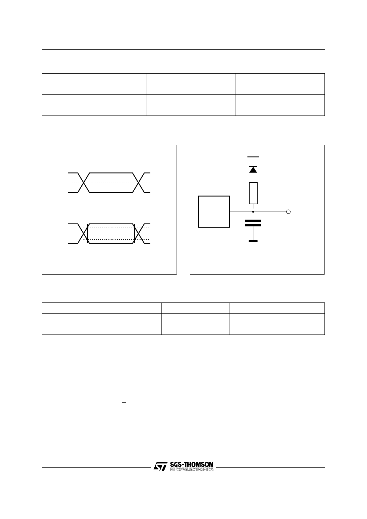
T ab le 5. AC Measurement Con ditions
High Speed Standard
Input Rise and Fall Times ≤ 10ns ≤ 20ns
Input Pulse Voltages 0 to 3V 0.4V to 2.4V
Input and Output Timing Ref. Voltages 1.5V 0.8V and 2V
Figure 3. AC Test ing Input Outp ut W avefo rm
High Speed
3V
1.5V
0V
Standard
2.4V
0.4V
T ab le 6. Capacitance
Symbol Parameter Test Condition Min Max Unit
C
IN
C
OUT
Note: 1. Sampled only , not 100% tested.
(1)
(TA = 25 °C, f = 1 MHz )
Input Capacitance VIN = 0V 6 pF
Output Capacitance V
2.0V
0.8V
AI01822
Figure 4. AC T est ing Load Circu it
1.3V
1N914
3.3kΩ
DEVICE
UNDER
TEST
CL = 30pF or 100pF
CL = 30pF for High Speed
CL = 100pF for Standard
CL includes JIG capacitance
= 0V 12 pF
OUT
OUT
AI01823
System Consi der atio n s
The power switching characteristics of Advance
CMOS EPROMs require careful decoupling of the
devices. The supply current, I
, has three seg-
CC
ments that are of interest to the system designer:
the standby current level, the active current level,
and transient current peaks that are produced by
the falling and rising edges of
E. The magnitude of
this transient current peaks is dependent on the
capacitive and inductive loading of the device at the
output. The associated transient vo ltage peaks can
be suppressed by complying with the two line
4/13
output control and by properly select ed decoupling
capacitors. It is recommended that a 0.1µF ceramic
capacitor be used on every device between V
CC
and VSS. This should be a high frequency capacitor
of low inherent inductance and should be placed
as close to the device as possible. In addition, a
4.7µF bulk electrolytic capacitor should be used
between V
and VSS for every eight devices. The
CC
bulk capacitor should be located near the power
supply connection point. The purpose of the bulk
capacitor is to overcome the voltage drop caused
by the inductive effects of PCB trac es.
 Loading...