

SGS Thomson Microelectronics M74HCT75TTR, M74HCT75RM13TR, M74HCT75M1R, M74HCT75B1R Datasheet
M74HCT75
4 BIT D TYPE LATCH
■ HIGH SPEED :
t
= 21ns (TYP.) at VCC = 4.5V
PD
■ LOW POWER DISSIPATION:
I
=2µA(MAX.) at TA=25°C
CC
■ COMPA TIBLE WITH TTL OUTPUTS :
V
= 2V (MIN.) VIL = 0.8V (MAX)
IH
■ BALANCED PROPAGATION DELAYS:
t
≅ t
PLH
■ SYMMETRICAL OUTPUT IMPEDANCE:
|I
OH
■ PIN AND FUNCTION COMPATIBLE WITH
PHL
| = IOL = 4mA (MIN)
74 SERIES 75
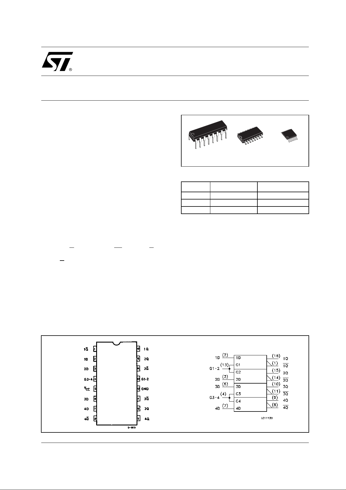
DESCRIPTION
The M74HCT75 is an high spe ed CMOS 4 BIT D
TYPE LATCH fabricated with silicon gate C
2
MOS
technology.
It contains two groups of 2 bit latches controlled by
an enable input (G1
•2 or G3•4). These two latch
groups can be used in different circuits. Each latch
has Q and Q
outputs (1Q - 4Q and 1Q - 4Q). The
data applied to the data input is transferred to the
Q and Q
outputs when the enable input is taken
high and the outputs will follow the data input as
long as the enable input is kept high. When the
TSSOPDIP SOP
ORDER CODES
PACKAGE TUBE T & R
DIP M74HCT75B1R
SOP M74HCT75M1R M74HCT75RM13TR
TSSOP M74HCT75TTR
enable input is taken low, the information data
applied to the data input is retained at the outputs.
The M74HCT75 is designed to directly interface
2
HSC
MOS systems with TTL and NMOS
components.
All inputs are equipped with protection circuits
against static discharge and transient excess
voltage.
PIN CONNECTION AND IEC LOGIC SYMBOLS
1/9September 2001
M74HCT75
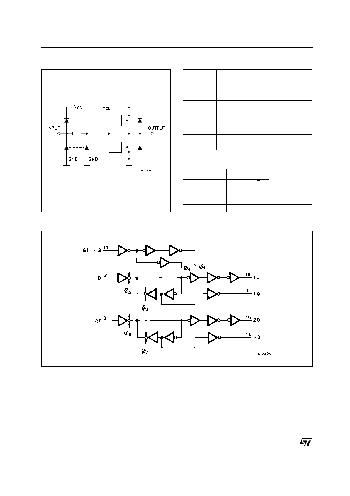
IINPUT AND OUTPUT EQUIVALENT CIRCUIT PIN DESCRIPTION
PIN No SYMBOL NAME AND FUNCTION
1, 4, 11, 8 1Q
2, 3, 6, 7 1D to 4D Data Inputs
4G3 • 4
13 G1 • 2
16, 15, 10, 9 1Q to 4Q Latch Outputs
12 GND Ground (0V)
5
TRUTH TABLE
to 4Q
V
CC
Complementary Latch
Outputs
Latch Enable Input,
latches 3 and 4
Latch Enable Input,
latches 1 and 2
Positive Supply Voltage
LOGIC DIAGRAM
INPUTS OUTPUTS
DGQQ
LHLH
HHHL
X L Qn Q
nLATCH
FUNCTION
2/9
M74HCT75
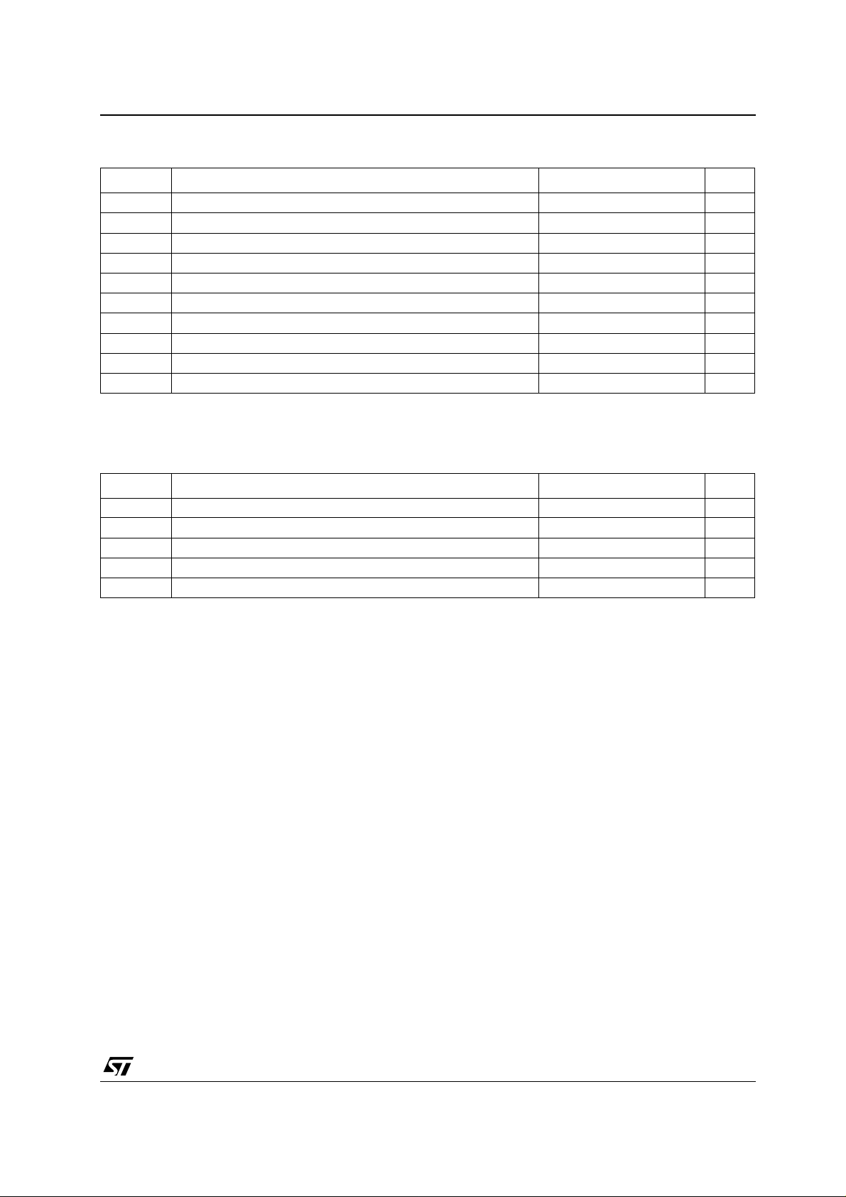
ABSOLUTE MAXIMUM RATINGS
Symbol Parameter Value Unit
V
V
V
I
I
OK
I
I
or I
CC
P
T
T
Absolute Maximum Ratings are those values beyond which damage to the device may occur. Functional operation under these conditions is
not implied
(*) 500mW at 65
RECOMMENDED OPERATING CONDITIONS
Symbol Parameter Value Unit
V
V
V
T
t
r
Supply Voltage
CC
DC Input Voltage -0.5 to VCC + 0.5
I
DC Output Voltage -0.5 to VCC + 0.5
O
DC Input Diode Current
IK
DC Output Diode Current
DC Output Current
O
DC VCC or Ground Current
GND
Power Dissipation
D
Storage Temperature
stg
Lead Temperature (10 sec)
L
°C; derate to 300mW by 10mW/°C from 65°C to 85°C
Supply Voltage
CC
Input Voltage 0 to V
I
Output Voltage 0 to V
O
Operating Temperature
op
, t
Input Rise and Fall Time (VCC = 4.5 to 5.5V)
f
-0.5 to +7 V
± 20 mA
± 20 mA
± 25 mA
± 50 mA
500(*) mW
-65 to +150 °C
300 °C
4.5 to 5.5 V
CC
CC
-55 to 125 °C
0 to 500 ns
V
V
V
V
3/9
 Loading...