

SGS Thomson Microelectronics M74HCT688 Datasheet

.HIGH SPEED
tPD= 17 ns(TYP.) AT VCC=5V
.LOWPOWER DISSIPATION
ICC=4µA(MAX.) AT TA=25°C
.COMPATIBLE WITH TTL OUTPUTS
VIH= 2V (MIN.) VIL= 0.8V (MAX)
.OUTPUT DRIVE CAPABILITY
10 LSTTLLOADS
.SYMMETRICALOUTPUT IMPEDANCE
|IOH|=IOL= 4 mA (MIN.)
.BALANCEDPROPAGATION DELAYS
t
PLH=tPHL
.PIN ANDFUNCTION COMPATIBLE
WITH 54/74LS688
M54HCT688
M74HCT688
8 BITEQUALITY COMPARATOR
B1R
(PlasticPackage)
M1R
(MicroPackage)
ORDER CODES :
M54HC T688F1R M74H CT688M1R
M74HC T688B1R M74HCT688C1R
F1R
(CeramicPackage)
C1R
(Chip Carrier)
DESCRIPTION
The M54/74HCT688 utilizes silicon gate C2MOS
technology to achieve operating speeds equivalent
to LSTTL devices. Along with the low power
dissipation and high noise immunity of standard
C2MOS integrated circuit, it possesses the driving
capability of 10 LSTTL load. The M54/74HCT688
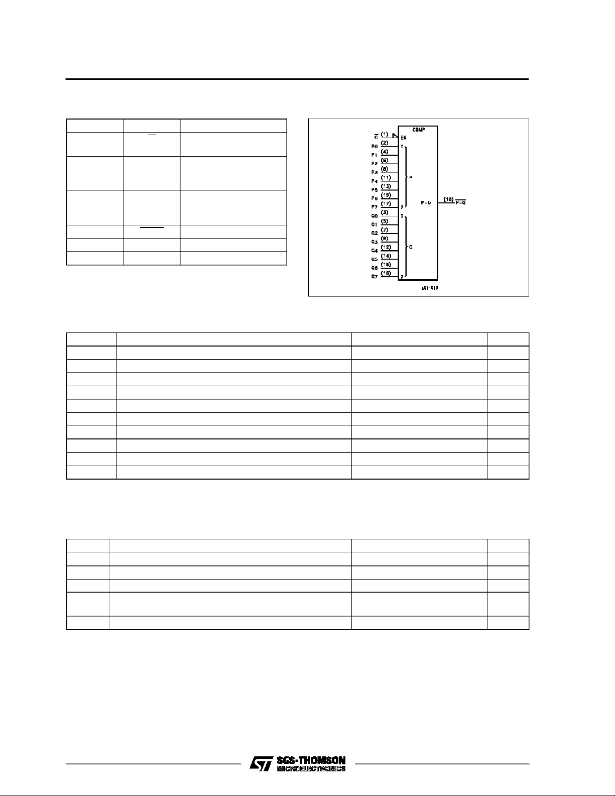
compares bitforbittwo8-bit wordsapplied oninputs
P0 - P7 and inputs Q0 - Q7 and indicates whether
or not they are equal. A single active lowenable is
provided to facilitate cascading severalpackagesto
enablecomparison of wordsgreater than 8 bits.
This integrated circuit has input and output
characteristics that are fully compatible with 54/74
LSTTL logic families. M54/74HCT devices are
designed to directly interface HSC2MOS systems
with TTL and NMOS components. They are also
plug in replacements for LSTTL devices giving a
reduction ofpower consumption.
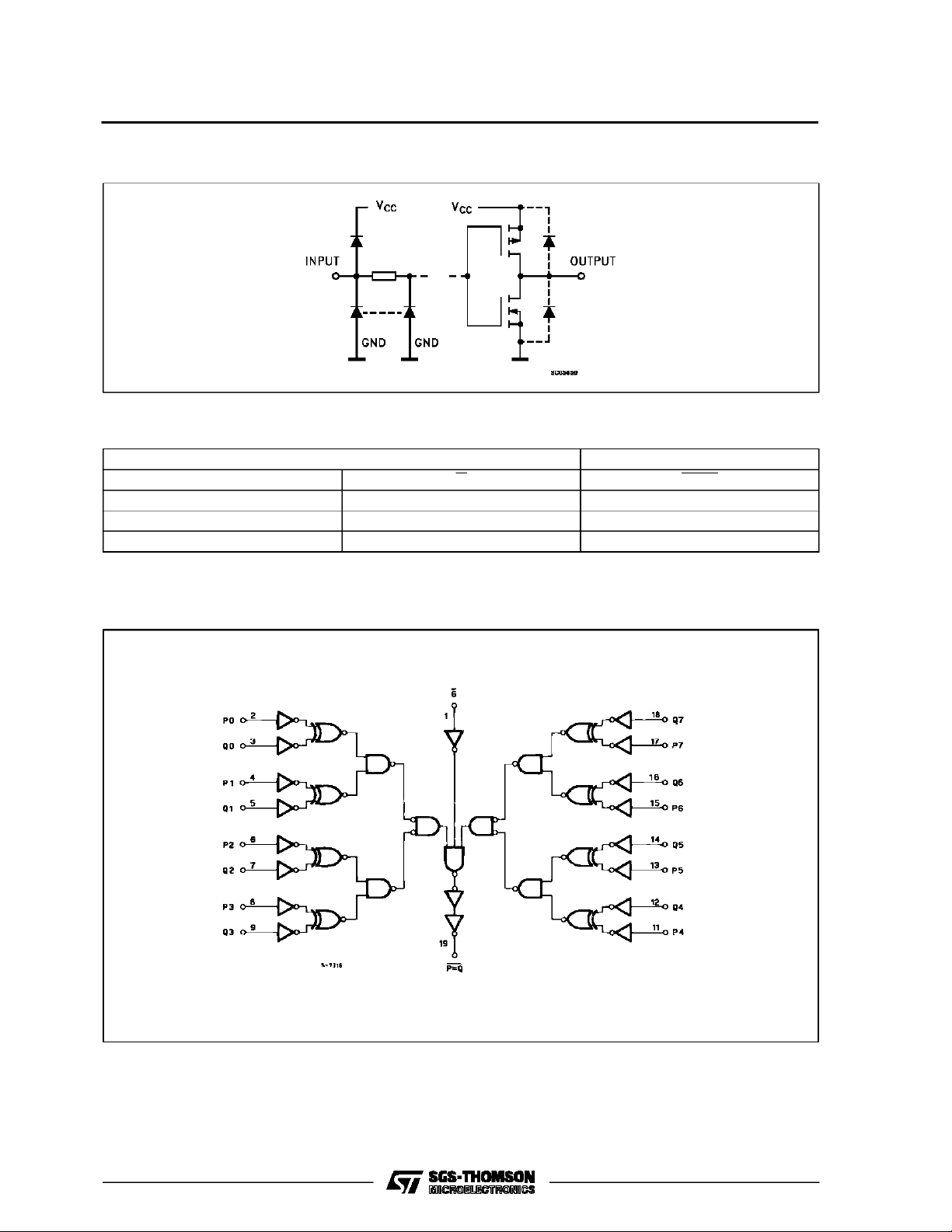
All inputs are equipped with protection circuit
against static discharge and transient excess
voltage.
PIN CONNECTIONS(top view)
NC =
No Internal
Connection
February 1993
1/10
M54/M74HCT688
INPUT AND OUTPUT EQUIVALENT CIRCUIT
TRUTH TABLE
INPUT OUTPUT
P, Q G P = Q
P=Q L L
P≠QL H
XHH
X:DON’T CARE
LOGIC DIAGRAM
2/10
M54/M74HCT688
PIN DESCRIPTION
IEC LOGIC SYMBOL
PIN No SYMBOL NAME AND FUNCTION
1 G Enable Input (Active
LOW)
2, 4, 6, 8,
P0 to P7 Word Inputs
11, 13, 15,
17
3, 5, 7, 9,
Q0 to Q7 Word Outputs
12, 14, 16,
18
19 P = Q Equal to Output
10 GND Ground (0V)
20 V
CC
Positive Supply Voltage
ABSOLU TE MAXIMU M RAT ING S
Symbol Parameter Value Unit
V
CC
V
V
O
I
IK
I
OK
I
O
or I
I
CC
P
D
T
stg
T
AbsoluteMaximumRatingsarethosevaluesbeyondwhichdamage tothedevicemayoccur.Functionaloperationunder theseconditionisnotimplied.
(*)500 mW:≅ 65oC derateto 300 mWby 10mW/oC: 65oCto85oC
Supply Voltage -0.5 to +7 V
DC Input Voltage -0.5 to VCC+ 0.5 V
I
DC Output Voltage -0.5 to VCC+ 0.5 V
DC Input Diode Current ± 20 mA
DC Output Diode Current ± 20 mA
DC Output Source Sink Current Per Output Pin ± 25 mA
DC VCCor Ground Current ± 50 mA
GND
Power Dissipation 500 (*) mW
Storage Temperature -65 to +150
Lead Temperature (10 sec) 300
L
o
C
o
C
RECO MM ENDED OPERATIN G CONDI TI O NS
Symbol Parameter Value Unit
V
T
t
V
V
r,tf
Supply Voltage 4.5 to 5.5 V
CC
Input Voltage 0 to V
I
Output Voltage 0 to V
O
Operating Temperature: M54HC Series
op
M74HC Series
CC
CC
-55 to +125
-40 to +85
Input Rise and Fall Time (VCC= 4.5 to 5.5V) 0 to 500 ns
V
V
o
C
o
C
3/10
 Loading...