

SGS Thomson Microelectronics M74HCT652, M74HCT651 Datasheet
M74HCT651
M74HCT652
HCT651 OCTAL BUS TRANSCEIVER/REGISTER (3-STATE, INV.)
HCT652 OCTAL BUS TRANSCEIVER/REGISTER (3-STATE)
.HIGH SPEED
f
= 60 MHz (TYP.)AT VCC=5V
MAX
.COMPATIBLE WITHTTL OUTPUTS
VIH= 2 V (MIN.) AT VIL= 0.8V (MAX)
.LOWPOWER DISSIPATION
ICC=4µA(MAX) AT TA=25oC
.OUTPUTDRIVE CAPABILITY
15 LSTTL LOADS
.SYMMETRICAL OUTPUT IMPEDANCE
IOH =IOL= 6 mA (mIN.)
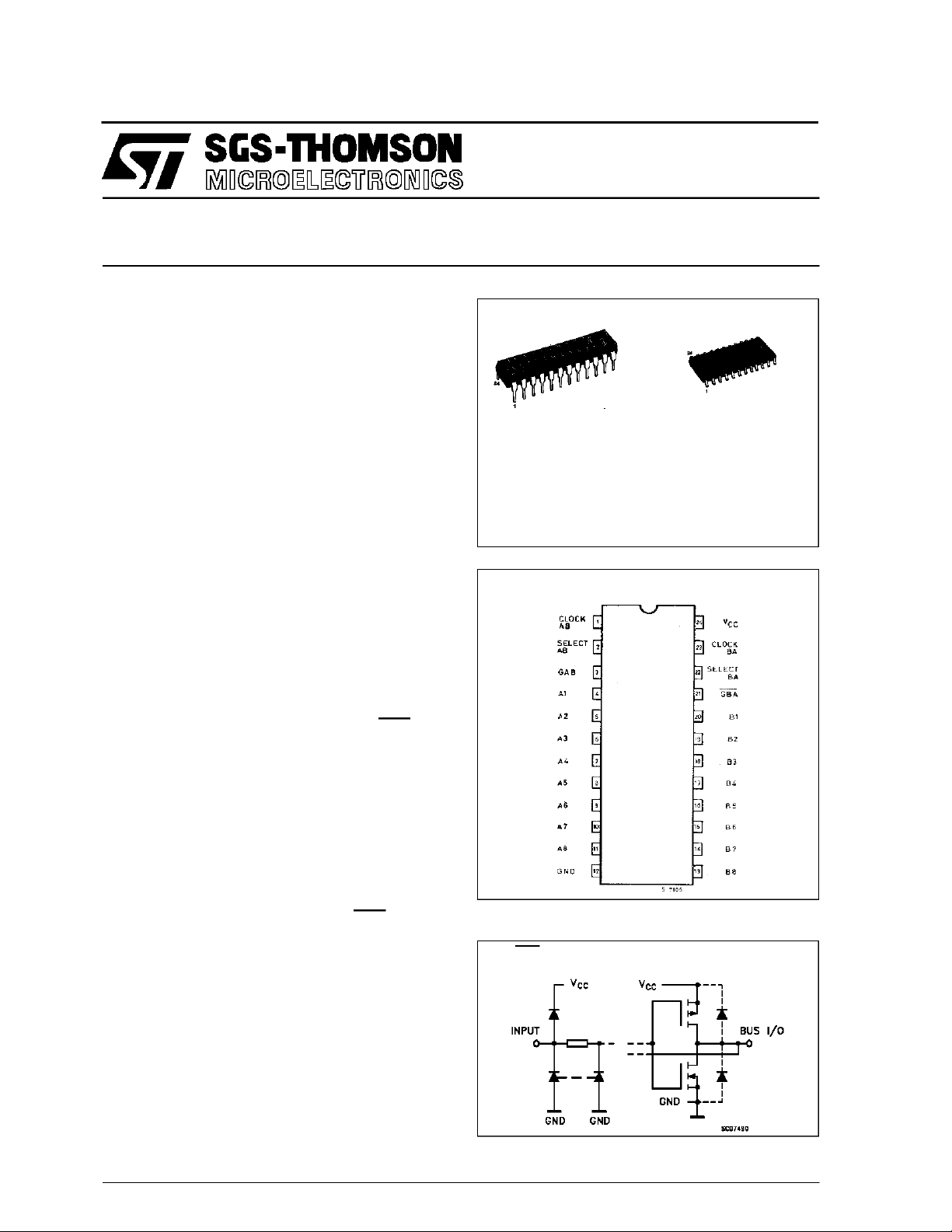
B1R
(PlasticPackage)
M1R
(MicroPackage)
.BALANCEDPROPAGATIONDELAYS
t
PLH=tPHL
.PIN ANDFUNCTION COMPATIBLE
WITH 54/74LS651/652
DESCRIPTION
M74HCT651/652 are high speed CMOS OCTAL
BUS TRANSCEIVERS AND REGISTERS
(3-STATE), fabricated in silicon gate C2MOS
technology. They have the same high speed
performance of LSTTL combined with true CMOS
low power consumption. These devices consist of
bustransceiver circuits, D-typeflip-flops, andcontrol
circuitry arranged for multiplexed transmission of
data directly from the input bus or from the internal
storage registers. Enable GAB and GBA are
provided to control the transceiverfunctions. Select
AB andSelect BA control pins are provided to select
whether real-time orstored dataistransfered. A low
input levelselectsreal-time data, anda high selects
stored data. Data onthe A or B bus, or both,can be
stored in the internal D flip-flops by low-to-high
transitionsattheappropriate clock pins(CLOCKAB
or CLOCK BA) regardless of the select or enable
controlpins.When select ABand selectBAareinthe
real-time transfer mode, it is also possible to store
data without using the internal D-type flip-flops by
simultaneously enabling GAB and GBA. In this
configuration each outputreinforces its input. Thus,
when all other data sources to the two sets of bus
linesareat highimpedance, eachset ofbuslineswill
remain at its last state. All inputs are equipped with
protection circuits against static discharge and
transient excess voltage.This integrated circuit has
input and output characteristics that are fully
compatible with 54/74 LSTTL logic families.
M54/74HCT devices are designed to directly
interface HSCMOS systems with TTL and NMOS
components. Theyare also plugin replacements for
LSTTL devices giving a reduction of power
consumption.
M74HC X XXM1R M74HC XXXB1R
PIN CONNECTIONS (top view)
INPUT AND OUTPUT EQUIVALENT CIRCUIT
GAB,GAB, CAB, A, B
SAB,SBA, CBA
ORDER CODES :
October 1993
1/12
M74HCT651/652
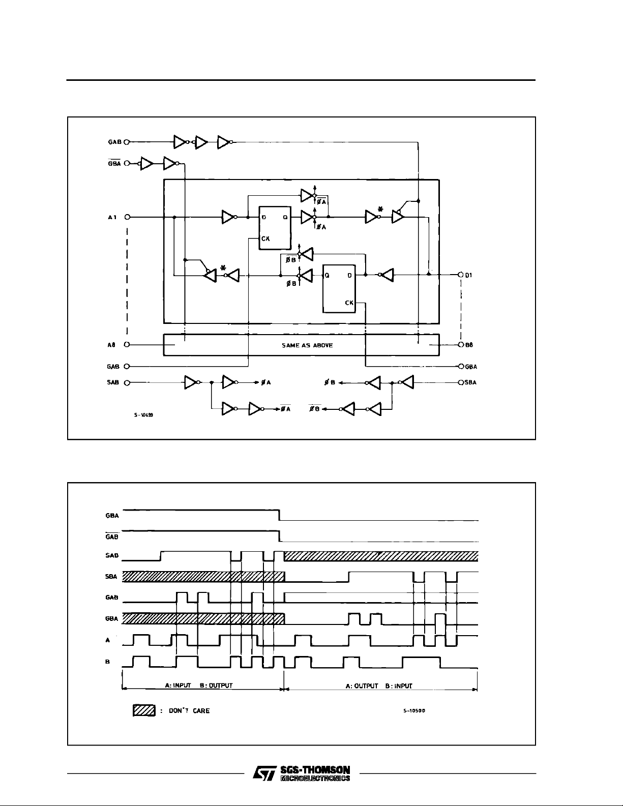
LOGIC DIAGRAM (HCT651)
Note: Incase of 74HCT652 outputinvertermarked *at A busand B bus are eliminated.
TIMING CHART
2/12
M74HCT651/652
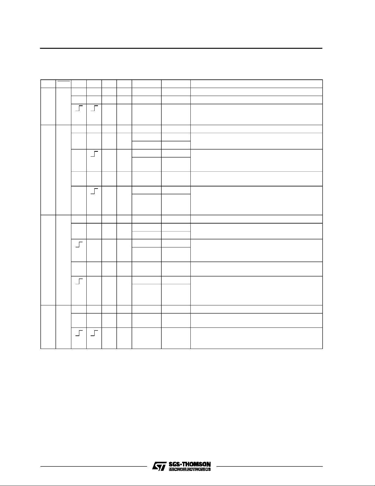
TRUTH TABLE
HCT652 (The tru th table for HC T651 is the same as this, but with th e o utputs invert ed)
GAB GBA CAB CBA SAB SBA A B FUNCTION
INPUTS INPUTS Both the A bus and the B bus are inputs
LH
LL
HH
HL
X : DON’TCARE
Z :HIGHIMPEDANCE
Qn :THE DATA STOREDTO THE INTERNALFLIP-FLOPSBY MOST RECENTLOWTO HIGH TRANSITIONOF THECLOCK INPUTS
* : THE DATAAT THE A AND B BUS WILLBE STORED TOTHE INTERNALFLIP-FLOPSON EVERY LOWTO HIGH TRANSITIONOF
THECLOCK INPUTS
X X X X Z Z The output functions of the A and B bus are disabled
X X INPUTS INPUTS Both the A and B bus are used for inputs to the
internal flip-flops. Data at the bus will be stored on
low to high transition of the clock inputs
OUTPUTS INPUTS The A bus are outputs and the B bus are inputs
X* X X L L L The data at the B bus are displayed at the A bus
HH
X* X L L L The data at the B bus ar displayed at the A bus.
HH
The data of the B bus are stored to the internal
flip-flop on low to high transition of th clock pulse
X* X X H Qn X The data stored to the internal flip-flop are dispayed
at the A bus
X* X H L L The data at the B bus are stored to the internal flip-
HH
flop on low to high transition of the clock pulse. The
states of the internal flip-flops output directly to the
A bus
INPUTS OUTPUTS The A bus are inputs and the B bus are outputs
XX*L X
L L The data at the A bus are displayed at the B bus
HH
X* L X L L The data at the A bus are displayed at the B bus.
HH
The data of the A bus are stored to the internal flipflop on low to high transition of the clock pulse
X X* H X X Qn The data stored to the internal flip-flops are
displayed at the B bus
X* H X L L the data at the A bus are stored to the internal flip-
HH
flop on low to high transition of the clock pulse. The
states of the internal flip-flops output directly to the
B bus
OUTPUTS OUTPUTS Both the A bus and the B bus are outputs
X X H H Qn Qn The data stored to the internal flip-flops are
displayed at the A and B bus respactively
H H Qn Qn The output at the A bus are displayed at the B bus,
the output at the B bus are displayed at the A bus
respectively
3/12
M74HCT651/652
PIN DESCRIPTION
PIN No SYMBOL NAME AND FUNCTION
1 CLOCK AB A to B Clock Input (LOW to HIGH, Edge-Trigged)
2 SELECT AB Select A to B Source Input
3 GAB Direction Control Input
4, 5, 6, 7, 8, 9, 10, 11 A1 to A8 A data Inputs/Outputs
20, 19, 18, 17, 16, 15, 14, 13 B1 to B8 B Data Inputs/Outputs
21 GBA Output Enable Input (Active LOW)
22 SELECT BA Select B to A Source Input
23 CLOCK BA B to A Clock Input (LOW to HIGH, Edge-Triggered)
12 GND Ground (0V)
24 V
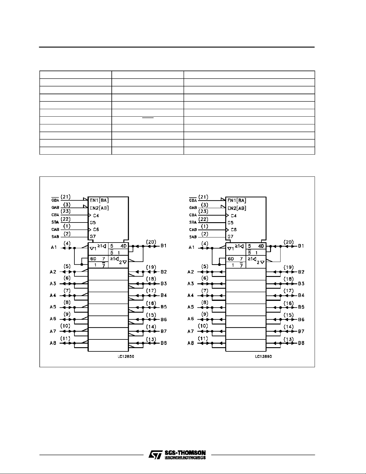
IEC LOGIC SYMBOLS
HCT651 HCT652
CC
Positive Supply Voltage
4/12
 Loading...