

SGS Thomson Microelectronics M74HCT648, M74HCT646 Datasheet
M74HCT646
M74HCT648
HCT646 OCTAL BUS TRANSCEIVER/REGISTER (3-STATE)
HCT648 OCTAL BUS TRANSCEIVER/REGISTER (3-STATE, INV.)
.HIGH SPEED
f
= 60 MHz(TYP.) AT VCC=5V
MAX
.LOWPOWERDISSIPATION
ICC=4µA(MAX.) AT TA=25°C
.COMPATIBLE WITHTTL OUTPUTS
VIH= 2V (MIN.)VIL= 0.8V (MAX)
.OUTPUT DRIVE CAPABILITY
15 LSTTL LOADS
B1R
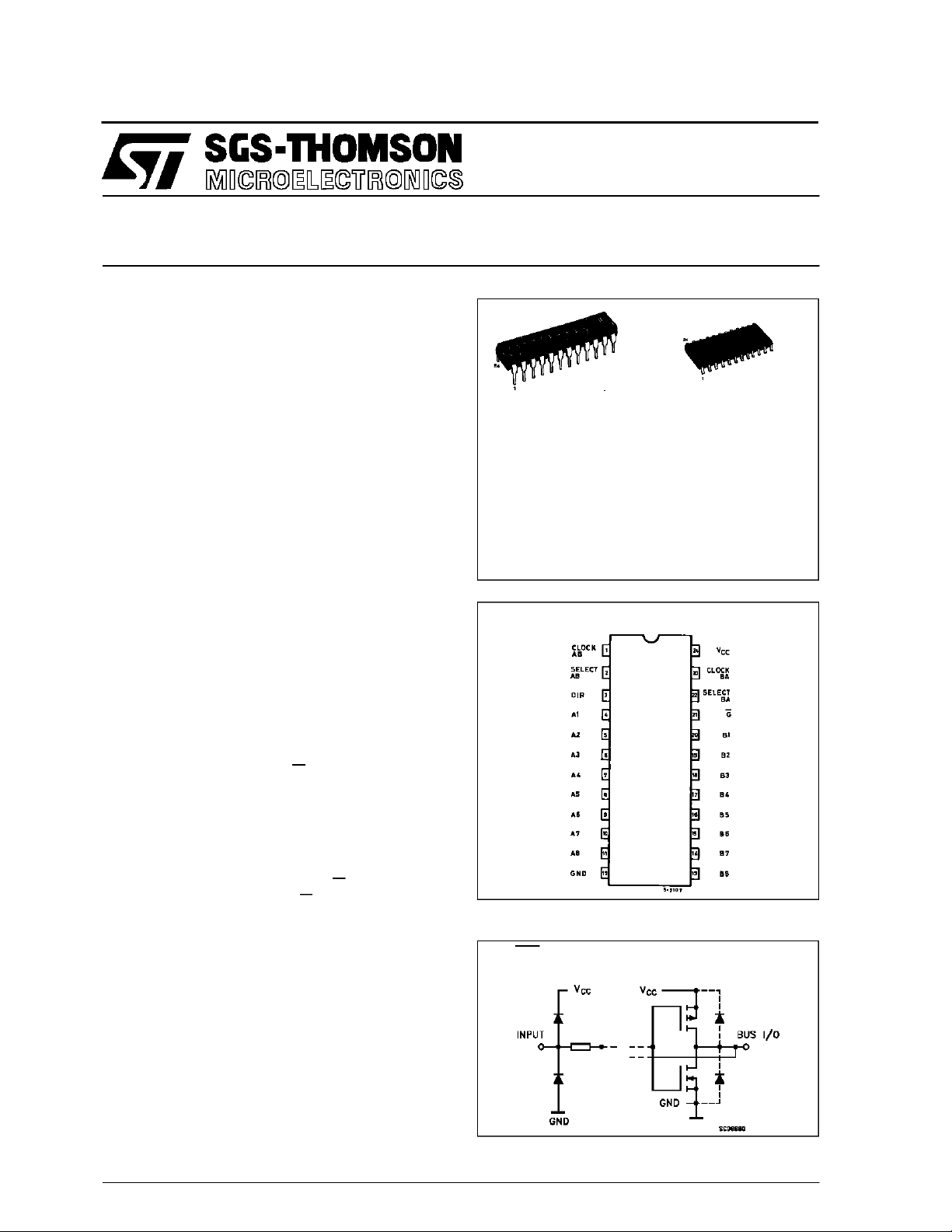
(PlasticPackage)
M1R
(Micro Package)
.SYMMETRICALOUTPUT IMPEDANCE
IOH=IOL=6 mA(MIN.)
.BALANCEDPROPAGATION DELAYS
t
PLH=tPHL
.PIN ANDFUNCTION COMPATIBLE
WITH 54/74LS646/648
DESCRIPTION
The M74HCT646/648 are high speed CMOS
OCTALBUS TRANSCEIVERS AND REGISTERS,
(3-STATE) fabricated in silicon gate C2MOS technology. They have the same high speed
performance of LSTTL combined with true CMOS
low power consumption. These devices consist of
bus transceiver circuits with 3-state output, D-type
flip-flops, and control circuitry arranged for multiplexed transmission of data directly from the input
bus or from the internal registers. Data on the A or
B bus will be clocked into the registers on thelowto-high transition of theappropriate clock pin (Clock
AB - or Clock BA). Enable (G) and direction (DIR)
pinsare providedtocontrolthe transceiverfunctions. In the transceiver mode, data present at the
high-impedanceportmay bestoredineitherregister
or inboth. Theselectcontrols (Select AB select BA)
can multiplex stored and real-time (transparent
mode)data. Thedirectioncontroldetermines which
bus willreceive data when enableG is active(low).
In theisolation mode (enable G high),”A” data may
be stored in one register and/or ”B” data may be
storedinthe otherregister.Whenanoutputfunction
is disabled, the input function is still enabled and
may be used to store and transmit data. Only one
of the two buses, A or B, may be driven at a time.
All inputs are equipped with protection circuits
against static discharge and transient excess voltage.This integrated circuit has input and output
characteristics that are fully compatible with 54/74
LSTTL logic families. M74HCT devices are designedto directly interfaceHSC2MOSsystemswith
TTLand NMOScomponents. Theyare also plug in
replacements for LSTTL devices giving areduction
of power consumption.
M74HC TXXXM1R M74H CTXX XB1R
PIN CONNECTIONS (top view)
INPUT AND OUTPUT EQUIVALENT CIRCUIT
GAB,GAB,CAB, A, B
SAB,SBA, CBA
ORDER CODES :
October 1993
1/12
M74HCT646/648
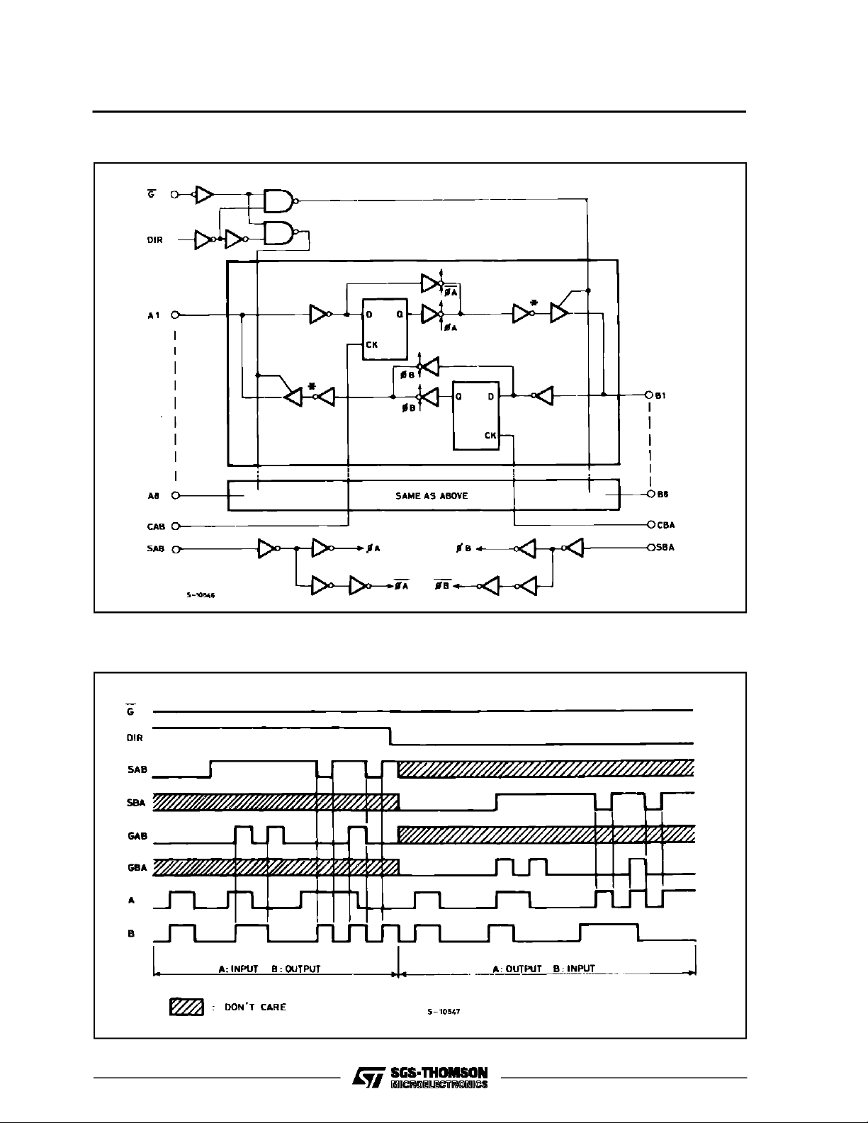
LOGIC DIAGRAM (HCT648)
Note: In case ofM54/74HCT646 output invertermarked *at A bus and B bus areeliminated.
TIMING CHART
2/12
M74HCT646/648
TRUTH TABLE
HCT646 (The trut h table for HCT64 8 is th e same as t his, but w i th t he o ut put s inver t ed)
G DIR CAB CBA SAB SBA A B FUNCTION
INPUTS INPUTS Both the A bus and the B bus are inputs
HX
LH
LL
X : DON’TCARE
Z :HIGH IMPEDANCE
Qn :THE DATA STOREDTO THE INTERNALFLIP-FLOPS BY MOST RECENT LOW TO HIGHTRANSITIONOF THE CLOCK INPUTS
* : THEDATA AT THE A ANDB BUSWILLBE STOREDTO THE INTERNALFLIP-FLOPSONEVERY LOW TO HIGH TRANSITIONOF
THECLOCK INPUTS
X X X X Z Z The output functions of the A and B bus are disabled
X X INPUTS INPUTS Both the A and B bus are used for inputs to the
internal flip-flops. Data at the bus will be stored on
low to high transition of the clock inputs
iNPUTS OUTPUTS The A bus are inputs and the B bus are outputs
X X* L X L L The data at the A bus are displayed at the B bus
HH
X* L X L L The data at the A bus are displayed at the B bus.
HH
The data of the A bus are stored to the internal
flip-flop on low to high transition of th clock pulse.
X X* H X X Qn The data stored to the internal flip-flop are dispayed
at the B bus
X* H X L L The data at the A bus are stored to the internal flip-
HH
flop on low to high transition of the clock pulse. The
states of the internal flip-flops output directly to the
B bus
OUTPUTS INPUTS The A bus are outputs and the B bus are inputs
X* X X L
L L The data at the B bus are displayed at the A bus
HH
X* X L L L The data at the B bus are displayed at the A bus.
HH
The data of the B bus are stored to the internal flipflop on low to high transition of the clock pulse
X* X X H Qn X The data stored to the internal flip-flops are
displayed at the B bus
x* X H L L the data at the B bus are stored to the internal flip-
HH
flop on low to high transition of the clock pulse. The
states of the internal flip-flops output directly to the
A bus
3/12
M74HCT646/648
PIN DESCRIPTION
PIN No SYMBOL NAME AND FUNCTION
1 CLOCK AB A to B Clock Input (LOW to HIGH, Edge-Trigged)
2 SELECT AB Select A to B Source Input
3 DIR Direction Control Input
4, 5, 6, 7, 8, 9, 10, 11 A1 to A8 A data Inputs/Outputs
20, 19, 18, 17, 16, 15, 14, 13 B1 to B8 B Data Inputs/Outputs
21 G Output Enable Input (Active LOW)
22 SELECT BA Select B to A Source Input
23 CLOCK BA B to A Clock Input (LOW to HIGH, Edge-Triggered)
12 GND Ground (0V)
24 V
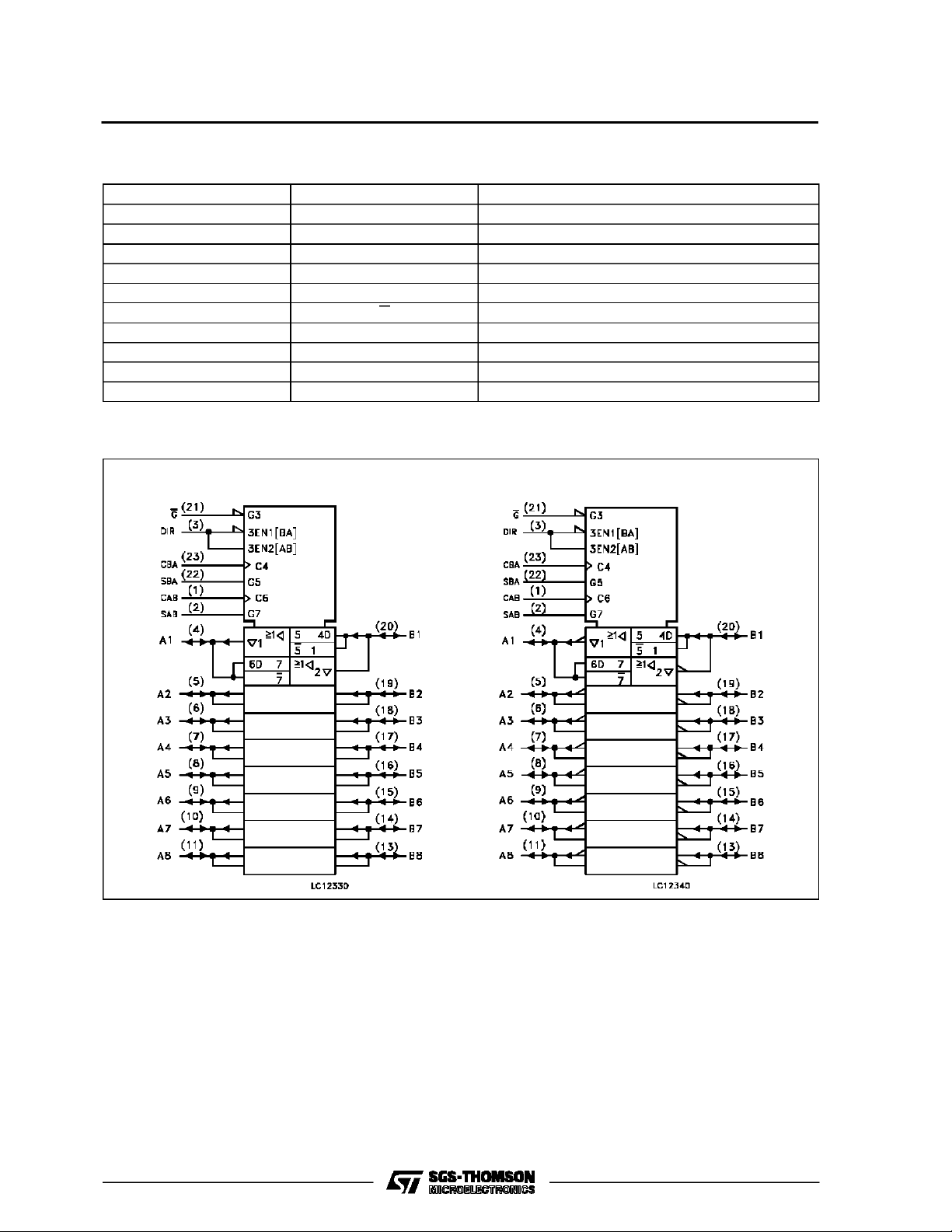
IEC LOGIC SYMBOLS
CC
HCT646 HCT648
Positive Supply Voltage
4/12
 Loading...