

SGS Thomson Microelectronics M74HCT573, M74HCT563 Datasheet
M54/74HCT563
M54/74HCT573
October1993
HCT563 INVERTING - HCT573 NONINVERTING
OCTAL D-TYPE LATCH WITH 3 STATE OUTPUT
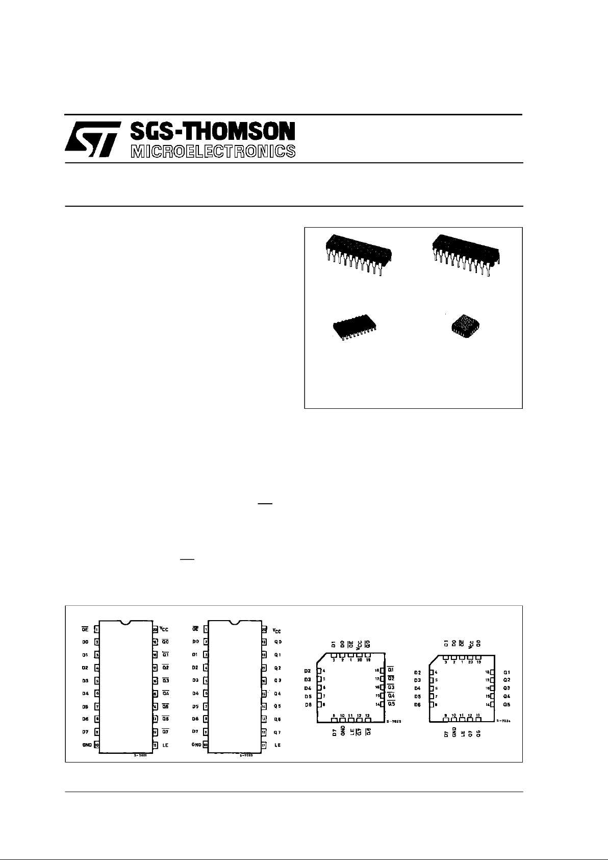
B1R
(PlasticPackage)
ORDER CODES :
M5 4HCT XXXF1R M74H CT X XXM1R
M74HCTX XX B1R M74HCTXXXC 1R
F1R
(CeramicPackage)
M1R
(MicroPackage)
C1R
(Chip Carrier)
PIN CONNECTION (top view)
.HIGH SPEED
tPD= 18 ns(TYP.) AT VCC=5V
.LOWPOWER DISSIPATION
ICC=4µA(MAX.) AT TA=25°C
.COMPATIBLE WITHTTL OUTPUTS
VIH= 2V (MIN.) VIL= 0.8V (MAX.)
.OUTPUTDRIVE CAPABILITY
15 LSTTL LOADS
.SYMMETRICAL OUTPUT IMPEDANCE
IOL=IOH= 6 mA (MIN.)
.BALANCEDPROPAGATIONDELAYS
t
PLH=tPHL
.PIN ANDFUNCTION COMPATIBLE
WITH 54/74LS563/573
DESCRIPTION
The M54/74HCT563 and M54HCT573 are high
speed CMOS OCTAL LATCH WITH 3-STATE
OUTPUTS fabricated with silicon gate C2MOS
technology.
These ICs achive the high speed operation similar
to equivalent LSTTL while maintaining the CMOS
low power dissipation.
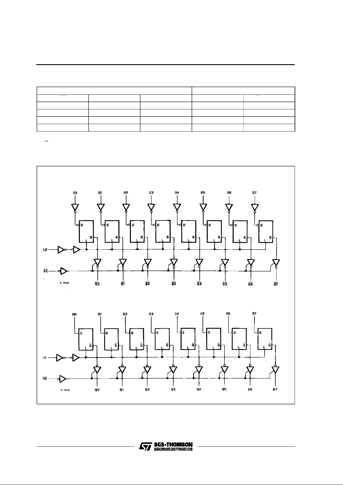
These8 bitD-Typelatchesare controlled by a latch
enable input (LE) and aoutput enable input (OE).
While the LE input is held at a high level, the Q
outputs will follow the data input precisely or
inversely. When the LE is taken low, the Q outputs
willbe latchedprecisely orinversely atthelogiclevel
of D input data. While the OE input is at low level,
the eightoutputs will be inanormal logicstate(high
or lowlogiclevel) andwhilehighlevel the outpts will
be in a high impedance state.
The application designer has a choise of
combination of invertingand non invertingoutputs.
This integrated circuit has input and output
characteristics that are fully compatible with 54/74
LSTTL logic families. M54/74HCT devices are
designed to directly interface HSC2MOS systems
with TTL and NMOS components. They are also
plug in replacements for LSTTL devices giving a
reduction of powerconsumption.
All inputs are equipped with protection circuits
against discharge and transient excessvoltage.
HCT563 HCT573 HCT563 HCT573
1/13

INPUT AND OUTPUT EQUIVALENT CIRCUIT
PIN DESCRIPTION (HCT 563)
PIN No SYMBOL NAME AND FUNCTION
1 OE 3 State output Enable
Input (Active LOW)
2, 3, 4, 5,
6, 7, 8, 9
D0 to D7 Data Inputs
12, 13, 14,
15, 16, 17,
18, 19
Q0 to Q7 3 State Latch Outputs
11 LE Latch Enable Input
10 GND Ground (0V)
20 V
CC
Positive Supply Voltage
PIN DESCRIPTIO N (HC T573)
PIN No SYMBOL NAME AND FUNCTION
1 OE 3 State output Enable
Input (Active LOW)
2, 3, 4, 5,
6, 7, 8, 9
D0 to D7 Data Inputs
12, 13, 14,
15, 16, 17,
18, 19
Q0 to Q7 3 State Latch Outputs
11 LE Latch Enable Input
10 GND Ground (0V)
20 V
CC
Positive Supply Voltage
IEC LOGIC SYMBOLS
HCT563 HCT573
M54/M74HCT563/573
2/13
TRUTH TABLE
INPUTS OUTPUTS
OE LE D Q (HCT573) Q (HCT563)
HXXZZ
L L X NO CHANGE * NO CHANGE *
LHLLH
LHHHL
X: DON’TCARE
Z: HIGHIMPEDANCE
*: Q/QOUTPUTSARE LATCHEDAT THE TIME WHENTHE LE INPUTIS TAKENLOW LOGIC LEVEL.
LOGIC DIAGRAMS
HCT563
HCT573
M54/M74HCT563/573
3/13
ABSOLU TE MAXIMU M R AT I NG S
Symbol Parameter Value Unit
V
CC
Supply Voltage -0.5 to +7 V
V
I
DC Input Voltage -0.5 to VCC+ 0.5 V
V
O
DC Output Voltage -0.5 to VCC+ 0.5 V
I
IK
DC Input Diode Current ± 20 mA
I
OK
DC Output Diode Current ± 20 mA
I
O
DC Output Source Sink Current Per Output Pin ± 35 mA
I
CC
or I
GND
DC VCCor Ground Current ± 70 mA
P
D
Power Dissipation 500 (*) mW
T
stg
Storage Temperature -65 to +150
o
C
T
L
Lead Temperature (10 sec) 300
o
C
AbsoluteMaximumRatingsarethosevaluesbeyondwhichdamage to thedevicemayoccur.Functionaloperationunder theseconditionisnotimplied.
(*)500 mW:≅ 65oC derate to 300 mW by 10mW/oC: 65oCto85oC
RECO MM ENDED O PERAT IN G CONDITIONS
Symbol Parameter Value Unit
V
CC
Supply Voltage 4.5 to 5.5 V
V
I
Input Voltage 0 to V
CC
V
V
O
Output Voltage 0 to V
CC
V
T
op
Operating Temperature: M54HC Series
M74HC Series
-55 to +125
-40 to +85
o
C
o
C
t
r,tf
Input Rise and Fall Time (VCC= 4.5 to 5.5V) 0 to 500 ns
M54/M74HCT563/573
4/13
 Loading...