

SGS Thomson Microelectronics M74HCT533, M74HCT373 Datasheet
OCTAL D-TYPE LATCH WITH3 STATE OUTPUT
HCT373 NON INVERTING - HCT533INVERTING
.HIGH SPEED
tPD= 17 ns(TYP.) AT VCC=5V
.LOWPOWER DISSIPATION
ICC=4µA(MAX.) AT TA=25°C
.COMPATIBLE WITHTTL OUTPUTS
VIH= 2V(MIN.) VIL= 0.8V (MAX.)
.OUTPUT DRIVE CAPABILITY
15 LSTTLLOADS
.SYMMETRICALOUTPUT IMPEDANCE
IOL=IOH= 6 mA (MIN.)
.BALANCEDPROPAGATION DELAYS
t
PLH=tPHL
.PIN AND FUNCTION COMPATIBLE
WITH 54/74LS373/533
DESCRIPTION
M54/74HCT373
M54/74HCT533
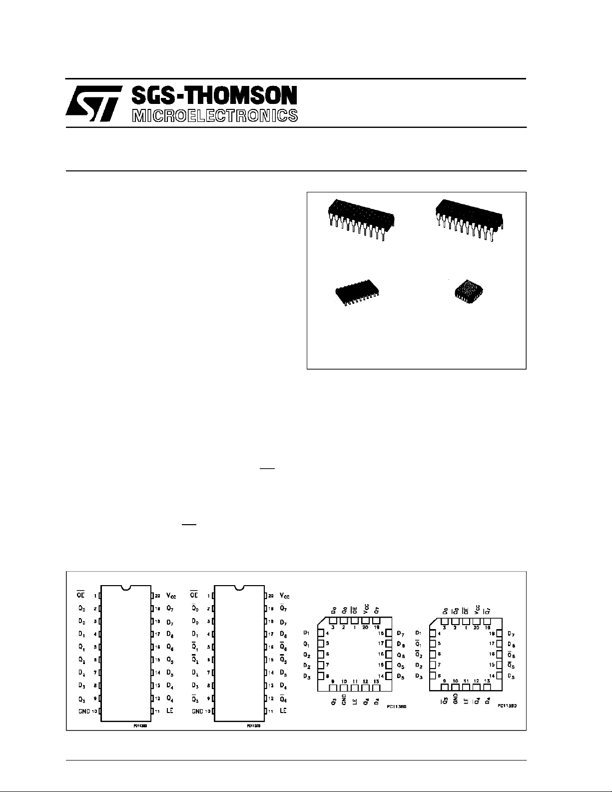
B1R
(PlasticPackage)
M1R
(MicroPackage)
ORDER CODES :
M54HCTXXX F1 R M74HCTXXXM 1R
M74HCTXXX B1R M74HCTX XXC1R
F1R
(CeramicPackage)
C1R
(Chip Carrier)
The M54/74HCT373 and M54HCT533 are high
speed CMOS OCTAL LATCH WITH 3-STATE
OUTPUTS fabricated with in silicon gate C2MOS
technology.
These ICs achive the high speed operation similar
to equivalent LSTTL while maintaning the CMOS
low power dissipation.
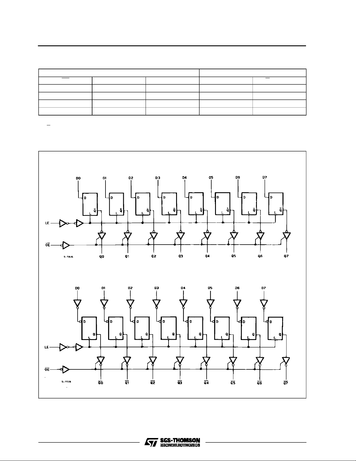
These8 bit D-Typelatchesare controlled bya latch
enable input(LE) and a output enable input (OE).
While the LE input is held at a high level, the Q
outputs will follow the data input precisely or
inversely. When the LE is taken low, the Q outputs
willbelatchedpreciselyorinversely atthelogiclevel
of D inputdata. While the OE inputis at low level,
the eight outputs will be inanormallogic state(high
PIN CONNECTION (top view)
HCT373 HCT533 HCT373 HCT533
or low logiclevel) andwhile high level the outptswill
be in a high impedance state. The application
designer has a choise of combination of inverting
and non inverting outputs. The three state output
configuration and the wide choise of outline make
bus organizedsystemsimple.
These integrated circuits have input and output
characteristics that are fully compatible with 54/74
LSTTL logic families. M54/74HCT devices are
designed to directly interface HSC2MOS systems
with TTL and NMOS components. They are also
plug in replacements for LSTTL devices giving a
reduction of power consumption. All inputs are
equipped with protection circuits against discharge
and transient excess voltage.
October 1993
1/13

M54/M74HCT373/533
INPUT AND OUTPUT EQUIVALENT CIRCUIT
PIN DESCRIPTION (HCT373)
PIN No SYMBOL NAME AND FUNCTION
1 OE 3 State output Enable
Input (Active LOW)
2, 5, 6, 9,
12, 15, 16,
19
3, 4, 7, 8,
13, 14, 17,
18
11 LE Latch Enable Input
10 GND Ground (0V)
20 V
Q0 to Q7 3 State outputs
D0 to D7 Data Inputs
CC
Positive Supply Voltage
IEC LOGIC SYMBOLS
HCT373 HCT533
PIN DESCRIPTION (H C T533 )
PIN No SYMBOL NAME AND FUNCTION
1 OE 3 State output Enable
Input (Active LOW)
2, 5, 6, 9,
12, 15, 16,
19
3, 4, 7, 8,
13, 14, 17,
18
11 LE Latch Enable Input
10 GND Ground (0V)
20 V
Q0 to Q7 3 State outputs
D0 to D7 Data Inputs
CC
Positive Supply Voltage
2/13
TRUTH TABLE
INPUTS OUTPUTS
OE LE D Q (HCT373) Q (HCT533)
HXXZZ
L L X NO CHANGE * NO CHANGE *
LHLLH
LHHHL
X: DON’T CARE
Z: HIGH IMPEDANCE
*: Q/Q OUTPUTS ARE LATCHED AT THE TIME WHEN THE LE INPUT IS TAKEN LOW LOGIC LEVEL.
LOGIC DIAGRAMS
HCT373
M54/M74HCT373/533
HCT533
3/13
M54/M74HCT373/533
ABSOLU TE MAXIMU M RATINGS
Symbol Parameter Value Unit
V
CC
V
V
O
I
IK
I
OK
I
O
I
or I
CC
P
D
T
stg
T
AbsoluteMaximumRatingsarethosevaluesbeyondwhichdamage tothedevicemayoccur.Functionaloperationunder theseconditionisnotimplied.
(*)500 mW: ≅ 65oC derateto300mW by 10mW/oC: 65oCto85oC
RECO MM ENDED O PERAT IN G CONDI TIONS
Symbol Parameter Value Unit
V
CC
V
I
V
O
T
op
t
r,tf
Supply Voltage -0.5 to +7 V
DC Input Voltage -0.5 to VCC+ 0.5 V
I
DC Output Voltage -0.5 to VCC+ 0.5 V
DC Input Diode Current ± 20 mA
DC Output Diode Current ± 20 mA
DC Output Source Sink Current Per Output Pin ± 35 mA
DC VCCor Ground Current ± 70 mA
GND
Power Dissipation 500 (*) mW
Storage Temperature -65 to +150
Lead Temperature (10sec) 300
L
Supply Voltage 4.5 to 5.5 V
Input Voltage 0 to V
Output Voltage 0 to V
Operating Temperature: M54HC Series
M74HC Series
CC
CC
-55 to +125
-40 to +85
Input Rise and Fall Time (VCC= 4.5 to 5.5V) 0 to 500 ns
o
C
o
C
V
V
o
C
o
C
4/13
 Loading...