

SGS Thomson Microelectronics M74HCT393 Datasheet
.HIGH SPEED
f
= 80 MHz(TYP.) ATVCC=5V
MAX
.LOWPOWER DISSIPATION
ICC=4µA(MAX.) AT TA=25°C
.COMPATIBLE WITHTTL OUTPUTS
VIH= 2V (MIN.) VIL= 0.8V (MAX)
.OUTPUT DRIVE CAPABILITY
10 LSTTL LOADS
.SYMMETRICALOUTPUT IMPEDANCE
|IOH|=IOL=4 mA (MIN.)
.BALANCEDPROPAGATION DELAYS
t
PLH=tPHL
.PIN AND FUNCTION COMPATIBLE
WITH 54/74LS393
M54HCT393
M74HCT393
DUAL BINARY COUNTER
B1R
(PlasticPackage)
M1R
(MicroPackage)
ORDER CODES :
M54HC T393F1R M74H CT393M1R
M74HC T393B1R M74HCT393C1R
F1R
(CeramicPackage)
C1R
(Chip Carrier)
DESCRIPTION
The M54/74HCT393is a high speed CMOSDUAL
BINARY COUNTER fabricated in silicon gate
C2MOS technology. It has the same high speed
performance of LSTTL combined with true COMS
low power consumption.
This counter circuit contains independent ripple
carry counters and two 4-bit ripple carry binary
counters, which can be cascated to create a single
divideby 256 counter.
Each4-bit counter isincremented on the hightolow
transition (negative edge) of the clock input,and
eachhas an independent clear input. When clearis
set to high all four bits of each counter are setto a
low level. This enables counttruncation and allows
the implementation of divide by N counter
configurations.
This integrated circuit has input and output
characteristics that are fully compatible with 54/74
LSTTL logic families. M54/74HCT devices are
designed to directly interface HSC2MOS systems
with TTL and NMOS components. They are also
plug in replacements for LSTTL devices giving a
reduction of power consumption.
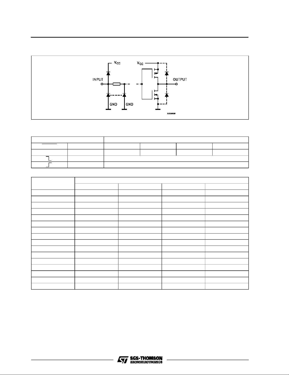
All inputs are equipped with protection circuits
against static discharge and transient excess
voltage.
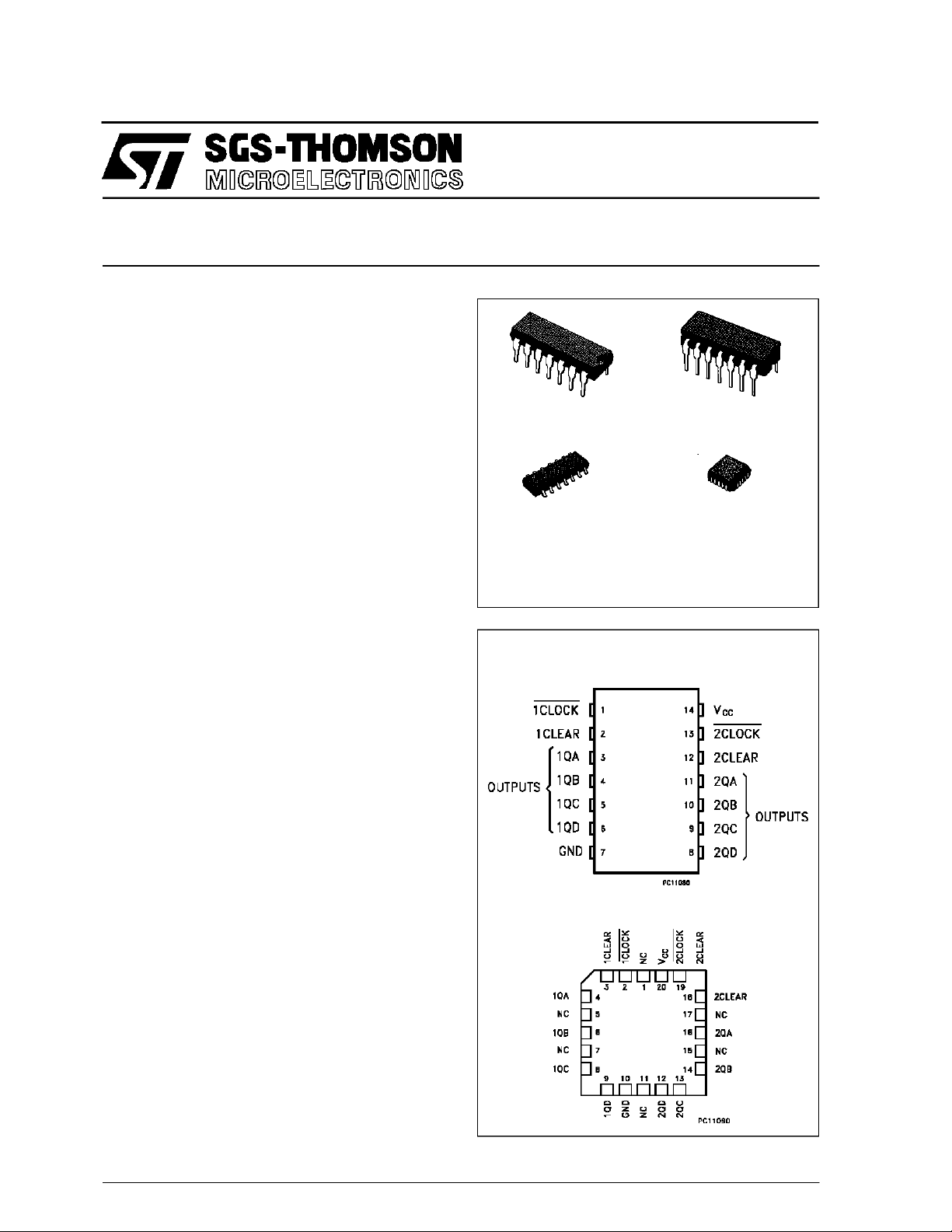
PIN CONNECTIONS(top view)
NC =
No Internal
Connection
October 1993
1/12
M54/M74HCT393
INPUT AND OUTPUT EQUIVALENT CIRCUIT
TRUTH TABLE
INPUTS OUTPUS
CLOCK CLEAR QD QC QB QA
XHLLLL
L COUNT UP
L NO CHANGE
X:Don’t Care
COUNT
0LLLL
1LLLH
2LLHL
3LLHH
4LHLL
5LHLH
6LHHL
7LHHH
8HLLL
9HLLH
10HLHL
11 H L H H
12 H H L L
13HHLH
14 H H H L
15HHHH
QD QC QB QA
OUTPUT
2/12
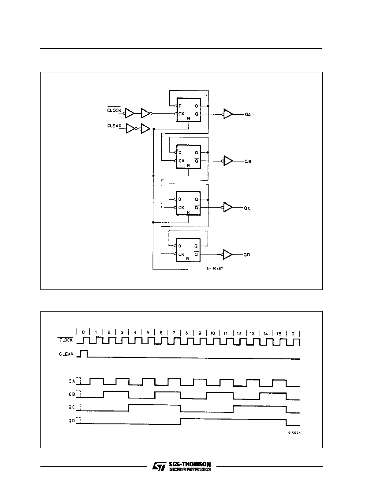
LOGI C DI AGRAM
M54/M74HCT393
TIM ING C HAR T
3/12
M54/M74HCT393
PIN DESCRIPTION
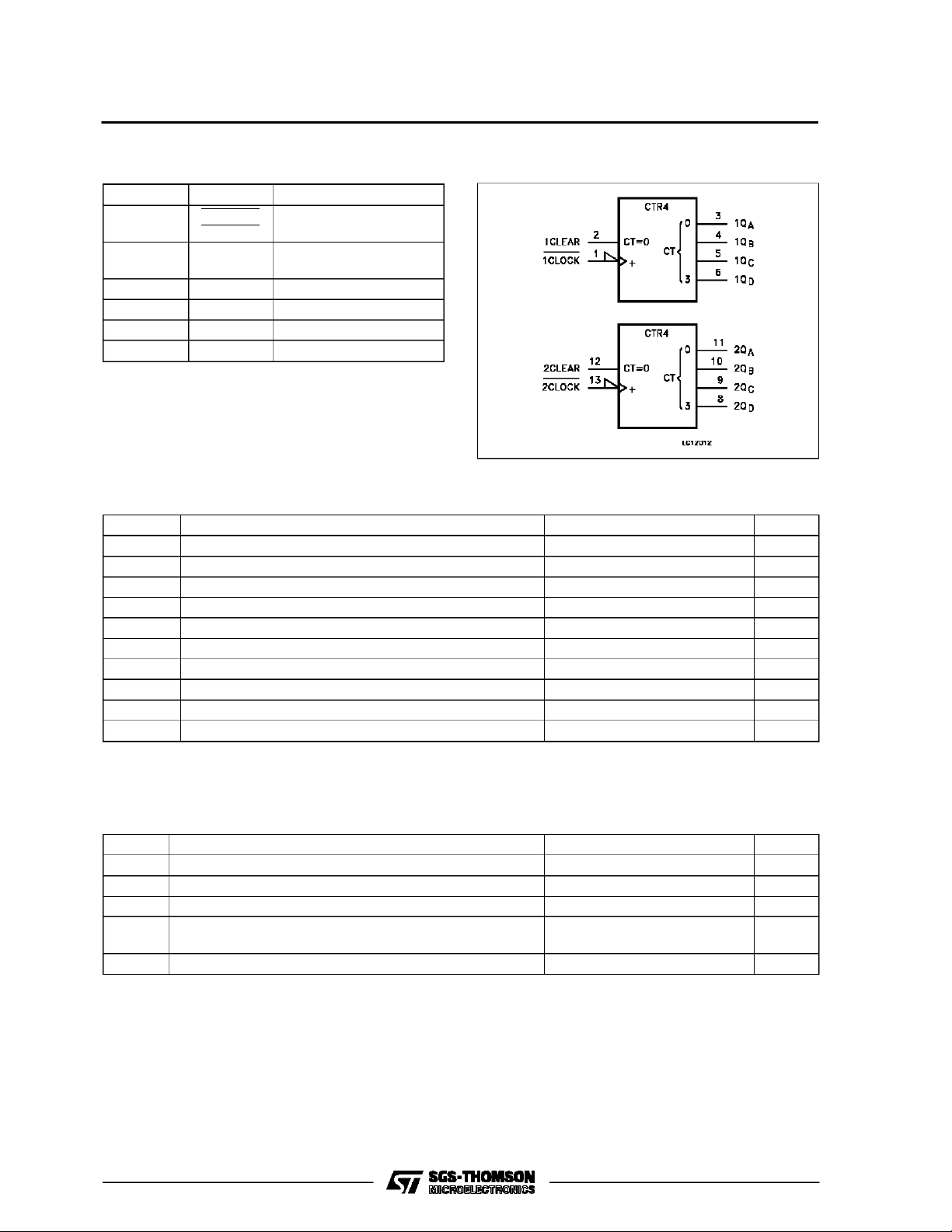
IEC LOGIC SYMBOL
PIN No SYMBOL NAME AND FUNCTION
1, 13 1 CLOCK
2 CLOCK
2, 12 1 CLEAR
2 CLEAR
Clock Input (HIGH to
LOW Edge triggered)
Asynchronouns Master
Reset Inputs
3, 4, 5, 6 1QA to 1QD Flip Flop Outputs
11, 10, 9, 8 2QA to 2QD Flip Flop Outputs
7 GND Ground (0V)
14 V
CC
Positive Supply Voltage
ABSOLU TE M AXIMU M R AT INGS
Symbol Parameter Value Unit
V
CC
V
V
O
I
IK
I
OK
I
O
or I
I
CC
P
D
T
stg
T
L
AbsoluteMaximumRatingsarethose values beyond whichdamagetothedevicemayoccur.Functional operation under theseconditionisnotimplied.
(*)500 mW: ≅ 65oC derate to300mW by 10mW/oC: 65oCto85oC
Supply Voltage -0.5 to +7 V
DC Input Voltage -0.5 to VCC+ 0.5 V
I
DC Output Voltage -0.5 to VCC+ 0.5 V
DC Input Diode Current ± 20 mA
DC Output Diode Current ± 20 mA
DC Output Source Sink Current Per Output Pin ± 25 mA
DC VCCor Ground Current ± 50 mA
GND
Power Dissipation 500 (*) mW
Storage Temperature -65 to +150
Lead Temperature (10 sec) 300
o
C
o
C
RECO MM ENDED OPERATI N G CO NDI TIONS
Symbol Parameter Value Unit
Supply Voltage 4.5 to 5.5 V
CC
Input Voltage 0 to V
I
Output Voltage 0 to V
O
Operating Temperature: M54HC Series
op
M74HC Series
CC
CC
-55 to +125
-40 to +85
Input Rise and Fall Time (VCC= 4.5 to 5.5V) 0 to 500 ns
4/12
V
T
t
V
V
r,tf
V
V
o
C
o
C
 Loading...