

SGS Thomson Microelectronics M74HCT374, M74HCT534 Datasheet
M54/74HCT374
M54/74HCT534
April1993
HCT374 NON INVERTING - HCT534INVERTING
OCTAL D-TYPE FLIP FLOP WITH 3 STATE OUTPUT
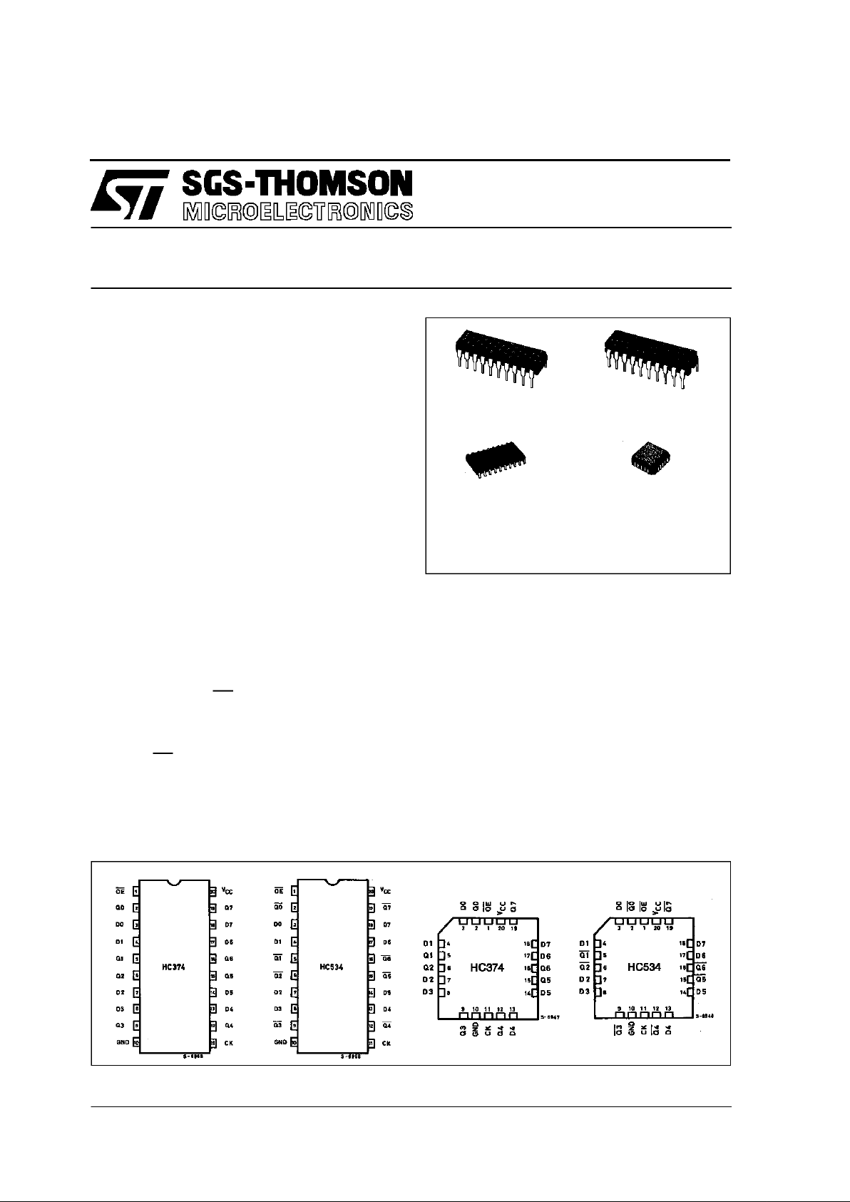
B1R
(PlasticPackage)
ORDER CODES :
M54HC T XXXF1R M74HC T XXXM1R
M74HC T XXXB1R M74HCTXXXC1R
F1R
(CeramicPackage)
M1R
(MicroPackage)
C1R
(Chip Carrier)
PIN CONNECTION (top view)
.HIGH SPEED
f
MAX
= 62 MHz(TYP.) AT VCC=5V
.LOWPOWER DISSIPATION
ICC=4µA(MAX.) AT TA=25°C
.COMPATIBLE WITHTTL OUTPUTS
VIH= 2V (MIN.)VIL= 0.8V (MAX)
.OUTPUT DRIVE CAPABILITY
15 LSTTL LOADS
.SYMMETRICAL OUTPUT IMPEDANCE
IOL=IOH= 6 mA (MIN.)
.BALANCEDPROPAGATION DELAYS
t
PLH=tPHL
.PIN AND FUNCTION COMPATIBLE
WITH 54/74LS374/534
DESCRIPTION
The M54/74HCT374, M54/74HCT534, are high
speed CMOSOCTALD-TYPEFLIPFLOP WITH 3STATE OUTPUTS fabricated with in silicon gate
C2MOS technology. They have the same high
speed performance of LSTTL combined with true
CMOS low power comsuption. These8-bit D-type
flip-flopsarecontrolled by a clockinput (CK)and an
ouput enable input (OE). On the positive transition
of the clock, the Q outputs will be set to the logic
state that were setup at the D inputs (HCT374) or
their complements (HCT534).
While the OEinput is low, the eight outputs will be
in a normal logic state (high or low logic level), and
while high level, the outputs willbe in a high impedancestate.Theoutputcontroldoesnotaffecttheinternaloperationofflip-flops.Thatis,theolddata can
be retained or the new data can be entered even
while the outputs are off. The application engineer
has a choice ofcombinationof inverting andnon-inverting outputs. The 3-state output configuration
and thewide choiceof outline make bus-organized
systemssimple.Allinputs areequipped withprotection circuits against static discharge and transient
excessvoltage. This integrated circuithas inputand
output characteristics that are fully compatible with
54/74 LSTTL logic families. M54/74HCT devices
are designed to directly interface HSC2MOS systems with TTL and NMOS components. They are
also plugin replacements for LSTTL devices giving
a reduction of power consumption.
1/13
INPUT AND OUTPUT EQUIVALENT CIRCUIT
PIN DESCRIPTION ( HCT374)
PIN No SYMBOL NAME AND FUNCTION
1 OE 3 State output Enable
Input (Active LOW)
2, 5, 6, 9,
12, 15, 16,
19
Q0 to Q7 3 State outputs
3, 4, 7, 8,
13, 14, 17,
18
D0 to D7 Data Inputs
11 CLOCK Clock Input (LOW to
HIGH, edge triggered)
10 GND Ground (0V)
20 V
CC
Positive Supply Voltage
PIN DESCRIPTIO N (HC T534 )
PIN No SYMBOL NAME AND FUNCTION
1 OE 3 State output Enable
Input (Active LOW)
2, 5, 6, 9,
12, 15, 16,
19
Q0 to Q7 3 State outputs
3, 4, 7, 8,
13, 14, 17,
18
D0 to D7 Data Inputs
11 CLOCK Clock Input (LOW to
HIGH, edge triggered)
10 GND Ground (0V)
20 V
CC
Positive Supply Voltage
IEC LOGIC SYMBOLS
HCT374 HCT534
M54/M74HCT374/534
2/13
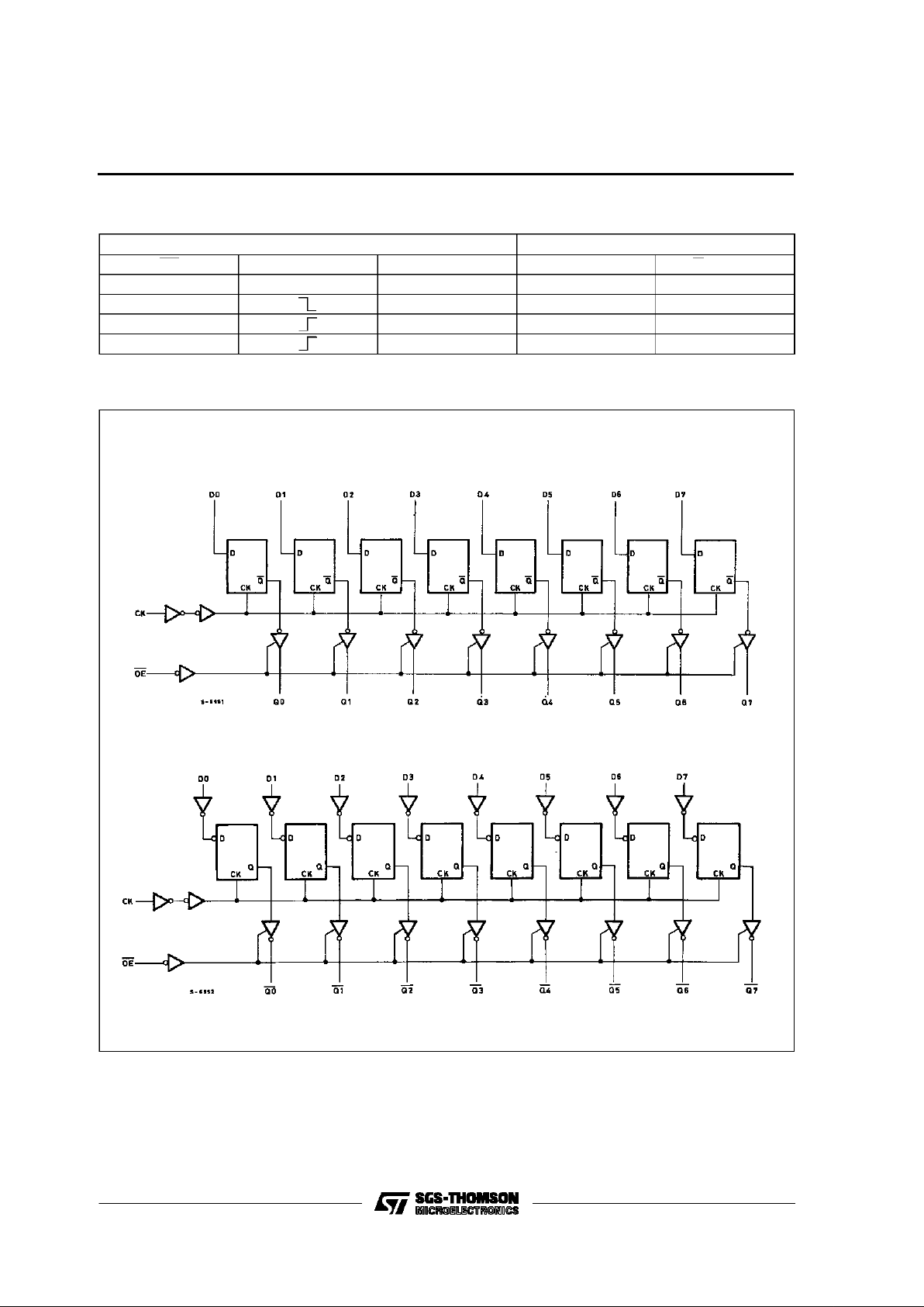
TRUTH TABLE
INPUTS OUTPUTS
OE CK D Q (HC374) Q (HC534)
HXXZZ
L X NO CHANGE NO CHANGE
LLLH
LHHL
LOGIC DIAGRAMS
HCT534
HCT374
M54/M74HCT374/534
3/13
ABSOLU TE MAXIMU M R AT I NG S
Symbol Parameter Value Unit
V
CC
Supply Voltage -0.5 to +7 V
V
I
DC Input Voltage -0.5 to VCC+ 0.5 V
V
O
DC Output Voltage -0.5 to VCC+ 0.5 V
I
IK
DC Input Diode Current ± 20 mA
I
OK
DC Output Diode Current ± 20 mA
I
O
DC Output Source Sink Current Per Output Pin ± 35 mA
I
CC
or I
GND
DC VCCor Ground Current ± 70 mA
P
D
Power Dissipation 500 (*) mW
T
stg
Storage Temperature -65 to +150
o
C
T
L
Lead Temperature (10 sec) 300
o
C
AbsoluteMaximumRatingsarethosevalues beyond whichdamage tothedevice mayoccur.Functionaloperationundertheseconditionisnotimplied.
(*)500 mW: ≅ 65oC derate to300mW by 10mW/oC: 65oCto85oC
RECO MM ENDED O PERAT IN G C O NDI TIONS
Symbol Parameter Value Unit
V
CC
Supply Voltage 4.5 to 5.5 V
V
I
Input Voltage 0 to V
CC
V
V
O
Output Voltage 0 to V
CC
V
T
op
Operating Temperature: M54HC Series
M74HC Series
-55 to +125
-40 to +85
o
C
o
C
t
r,tf
Input Rise and Fall Time (VCC= 4.5 to 5.5V) 0 to 500 ns
M54/M74HCT374/534
4/13
 Loading...