

SGS Thomson Microelectronics M74HCT32 Datasheet
.HIGH SPEED
tPD= 12 ns(TYP.) AT VCC=5V
.LOWPOWER DISSIPATION
ICC=1µA(MAX.) AT TA=25°C
.COMPATIBLE WITH TTL OUTPUTS
VIH= 2V (MIN.) VIL= 0.8V(MAX)
.OUTPUT DRIVE CAPABILITY
10 LSTTL LOADS
.SYMMETRICALOUTPUT IMPEDANCE
IOH =IOL= 4 mA (MIN.)
.BALANCEDPROPAGATION DELAYS
t
PLH=tPHL
.PIN AND FUNCTION COMPATIBLE WITH
54/74LS32
DESCRIPTION
TheM54/74HCT32 is a highspeedCMOS 2-INPUT
OR GATEfabricatedin silicongate C2MOS technology. It has the same high speed performance of
LSTTL combined with true CMOS low power consumption.Itachievesthehighspeedoperationsimilar
to equivalent LSTTL while maintaining the CMOS low
power dissipation. Theinternal circuit iscomposedof
2 stagesincluding buffered output, which gives high
noise immunity and a stable output. All inputs are
equipped with protection circuits against static discharge andtransient excessvoltage.
This integrated circuithas input and outputcharacteristicsthat are fully compatible with 54/74 LSTTL
logic families. M54/74HCT devices are designed to
directly interface HSC2MOS systemswith TTL and
NMOS components. They are also plug in replacements for LSTTL devices giving a reduction of
powerconsumption.
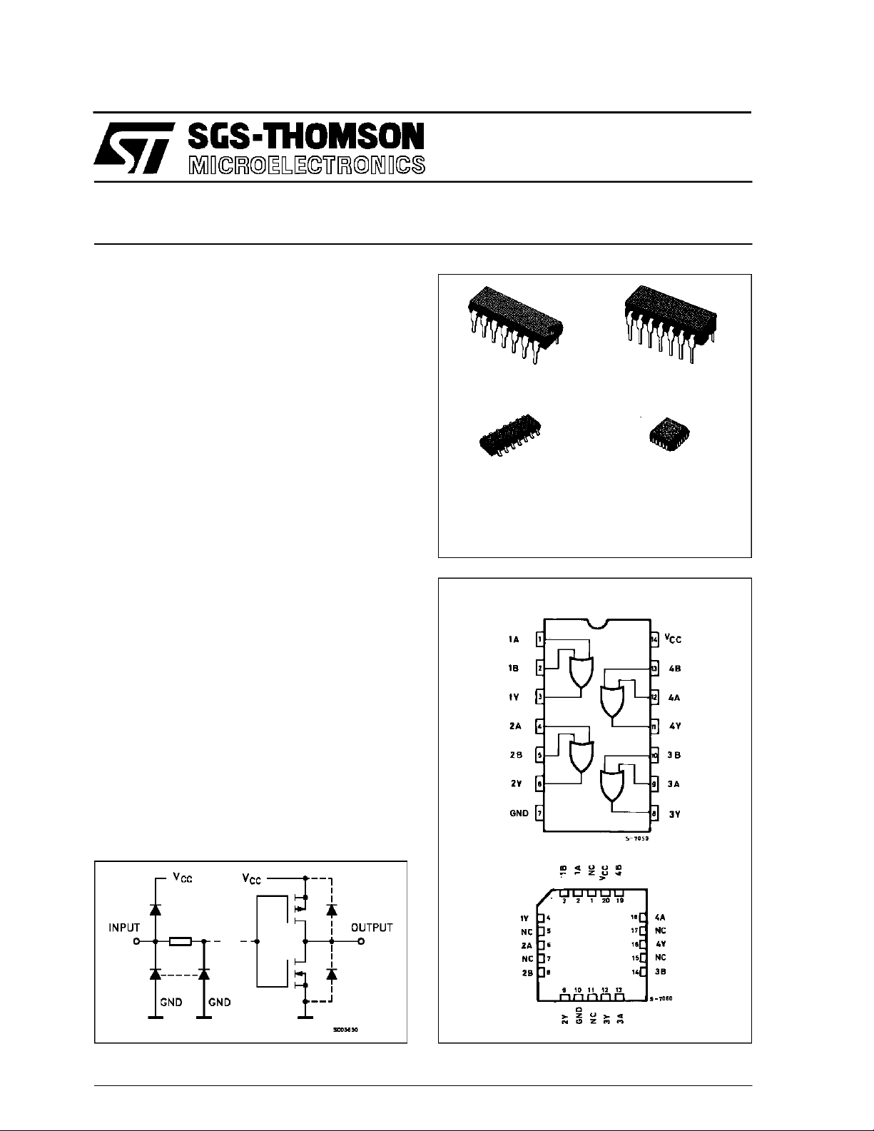
M54HCT32
M74HCT32
QUAD 2-INPUT OR GATE
B1R
(PlasticPackage)
M1R
(MicroPackage)
ORDER CODES :
M54HC T32F1R M74H CT32M1R
M74HC T32B1R M74HCT32C1R
PIN CONNECTIONS (top view)
F1R
(CeramicPackage)
C1R
(Chip Carrier)
INPUT AND OUTPUT EQUIVALENT CIRCUIT
February 1993
NC =
No Internal
Connection
1/9
M54/M74HCT32
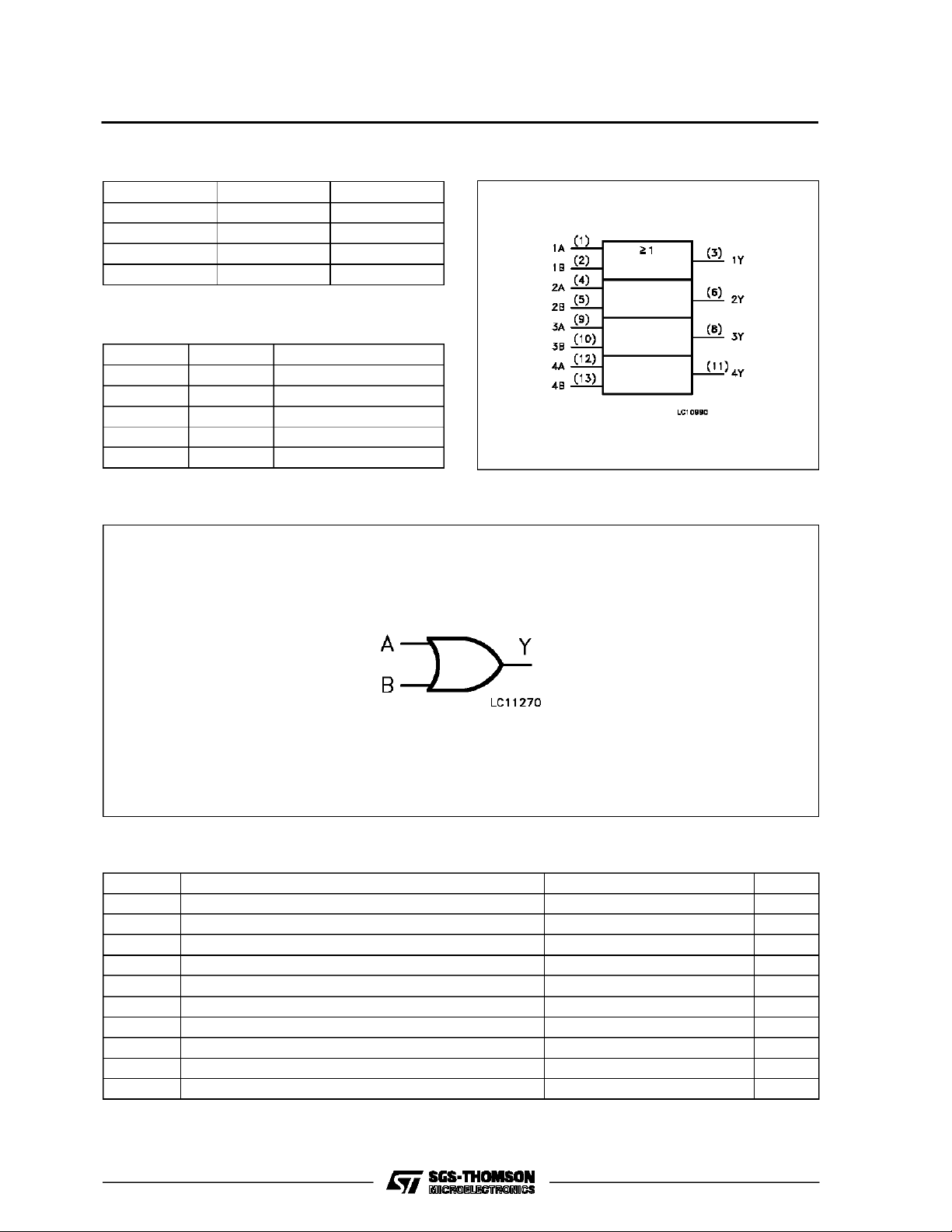
TRUTH TABLE
ABY
LLL
LHH
HLH
HHH
PIN DESCRIPTION
PIN No SYMBOL NAME AND FUNCTION
1, 4, 9, 12 1A to 4A Data Inputs
2, 5, 10, 13 1B to 4B Data Inputs
3, 6, 8, 11 1Y to 4Y Data Outputs
7 GND Ground (0V)
14 V
CC
Positive Supply Voltage
LOGI C DI AG RAM
IEC LOGIC SYMBOL
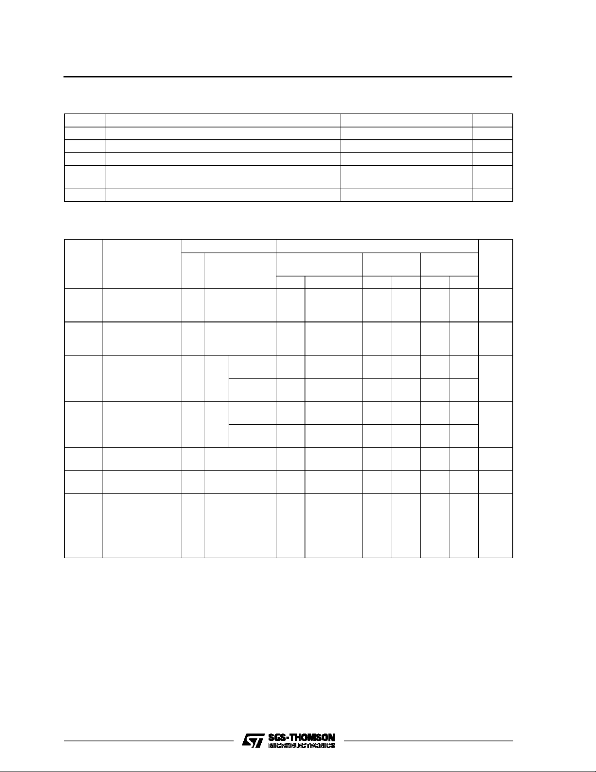
ABSOLU TE M AXIMU M R AT INGS
Symbol Parameter Value Unit
V
CC
V
V
O
I
IK
I
OK
I
O
or I
I
CC
P
D
T
stg
T
L
AbsoluteMaximumRatingsarethose values beyondwhichdamage tothedevice mayoccur. Functional operation under these conditionisnotimplied.
(*)500 mW:≅ 65oC derateto 300 mWby 10mW/oC: 65oCto85oC
2/9
Supply Voltage -0.5 to +7 V
DC Input Voltage -0.5 to VCC+ 0.5 V
I
DC Output Voltage -0.5 to VCC+ 0.5 V
DC Input Diode Current ± 20 mA
DC Output Diode Current ± 20 mA
DC Output Source Sink Current Per Output Pin ± 25 mA
DC VCCor Ground Current ± 50 mA
GND
Power Dissipation 500 (*) mW
Storage Temperature -65 to +150
Lead Temperature (10 sec) 300
o
C
o
C
M54/M74HCT32
RECO MM ENDED OPERAT IN G CO NDI TIONS
Symbol Parameter Value Unit
V
V
V
T
t
r,tf
DC SPECIFICATIONS
Symbol Parameter
V
V
V
OH
V
OL
I
I
CC
∆I
Supply Voltage 4.5 to 5.5 V
CC
Input Voltage 0 to V
I
Output Voltage 0 to V
O
Operating Temperature: M54HC Series
op
M74HC Series
CC
CC
-55 to +125
-40 to +85
Input Rise and Fall Time (VCC= 4.5 to 5.5V) 0 to 500 ns
Test Conditions Value
T
High Level Input
IH
Voltage
V
(V)
4.5
=25oC
CC
A
54HC and 74HC
Min. Typ. Max. Min. Max. Min. Max.
2.0 2.0 2.0 V
to
-40 to 85oC
74HC
-55 to 125oC
5.5
Low Level Input
IL
Voltage
4.5
to
0.8 0.8 0.8 V
5.5
High Level
Output Voltage
Low Level Output
Voltage
Input Leakage
I
Current
Quiescent Supply
VI=
IO=-20 µA 4.4 4.5 4.4 4.4
V
IH
4.5
or
I
=-4.0 mA 4.18 4.31 4.13 4.10
O
V
IL
VI=
IO=20µA 0.0 0.1 0.1 0.1
V
IH
4.5
or
I
= 4.0 mA 0.17 0.26 0.33 0.40
O
V
IL
VI=VCCor GND ±0.1 ±1 ±1 µA
5.5
5.5 VI=VCCor GND 1 10 20 µA
Current
Additional worst
CC
case supply
current
5.5 Per Input pin
V
= 0.5V or
I
VI= 2.4V
2.0 2.9 3.0 mA
Other Inputs at
VCCor GND
IO=0
54HC
V
V
o
C
o
C
Unit
V
V
3/9
 Loading...