

SGS Thomson Microelectronics M74HCT165 Datasheet
.HIGH SPEED
tPD= 17 ns(TYP.) AT VCC=5V
.LOWPOWER DISSIPATION
ICC=4µA(MAX.) AT TA=25°C
.OUTPUTDRIVE CAPABILITY
10 LSTTL LOADS
.BALANCEDPROPAGATION DELAYS
t
PLH=tPHL
.SYMMETRICALOUTPUT IMPEDANCE
IOL=IOH = 4 mA (MIN.)
.COMPATIBLE WITHTTL OUTPUTS
VIH= 2 V (MIN.) VIL= 0.8 V (MAX.)
.PIN AND FUNCTION COMPATIBLE
WITH 54/74LS165
DESCRIPTION
The M54/74HCT165 is a high speed CMOS 8 BIT
PISO SHIFT REGISTER fabricated in silicon gate
C2MOS technology. It has the same high speed
performance of LSTTL combined with true CMOS
low power consumption. It achives the high speed
operation similar to equivalent LSTTL while
maintaining the CMOS low power dissipation.
Thisdevice contains eight clockedmasterslave RS
flip-flopsconnected as a shiftregister,with auxiliary
gating to provide over-riding asynchronous parallel
entry.Parallel dataentrenswhenthe shift/loadinput
is low.Theparallel data canchange while shift/load
is low, provided that the recommended set-upand
hold times are observed. For clocked operation,
shift/loadmustbe high. The twoclockinputperform
identically; one can be used as a clock inhibit by
applying a high signal; to permit this operation
clocking is accomplished through a 2 input nor
gates.
Toavoiddoubleclocking,however,the inhibit signal
should only go high while the clock is high.
Otherwise the rising inhibit signal will cause the
same responseas risingclockedge.This integrated
circuit has input and output characteristics that are
fully compatible with 54/74 LSTTL logic families.
M54/74HCT devices are designed to directly
interface HSCMOS systems with TTL and NMOS
components.They arealsoplugin replacements for
LSTTL devices giving a reduction of power
consumption. All inputs are equipped with
protection circuits against static discharge and
transient excess voltage.
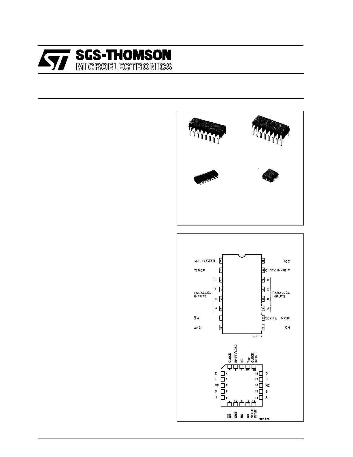
M54HCT165
M74HCT165
8 BITPISO SHIFT REGISTER
B1R
(PlasticPackage)
M1R
(MicroPackage)
ORDER CODES :
M54HC T165F1R M74H CT165M1R
M74HC T165B1R M74HCT165C1R
PIN CONNECTIONS(top view)
NC =
No Internal
Connection
F1R
(CeramicPackage)
C1R
(Chip Carrier)
October 1993
1/13
M54/M74HCT165
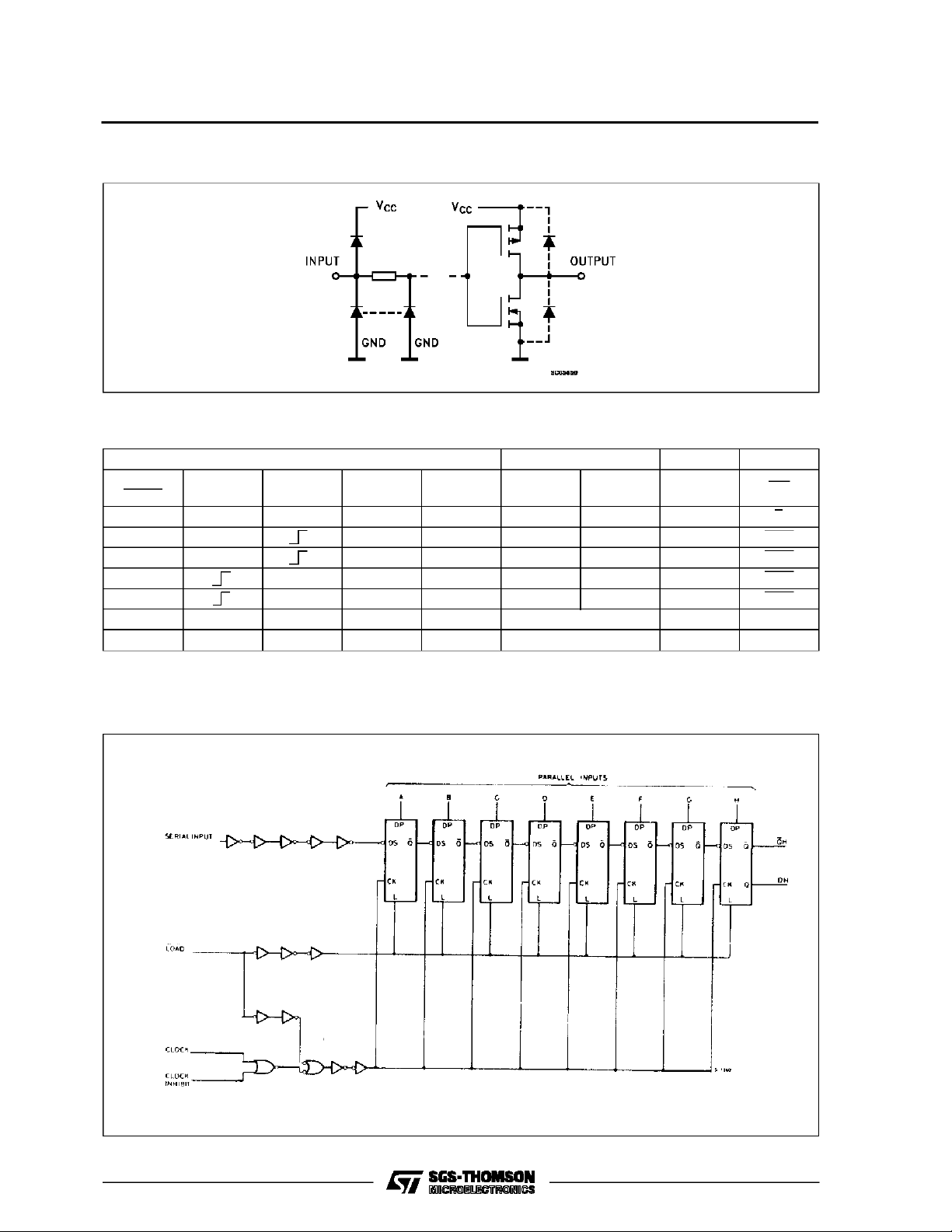
INPUT AND OUTPUT EQUIVALENT CIRCUIT
TRUTH TABLE
INPUTS INTERNAL OUTPUTS OUTPUS OUTPUS
SHIFT/
LOAD
L X X X a............h a b h h
H L H X H QAn QGn QGn
H L L X L QAn QGn QGn
H L H X H QAn QGn QGn
H L L X L QAn QGn QGn
H X H X X NO CHANGE
H H X X X NO CHANGE
a.......h:Thelevel of steadyinput voltage at inputs A throughH respectively
QAn- QGn : The levelof QA -QG,respectively, before themost-recent transitionof theclock.
CLOCK
INHIBIT
CLOCK SERIAL IN A .........H QA QB QH QH
LOGI C DI AGRAM
2/13
M54/M74HCT165
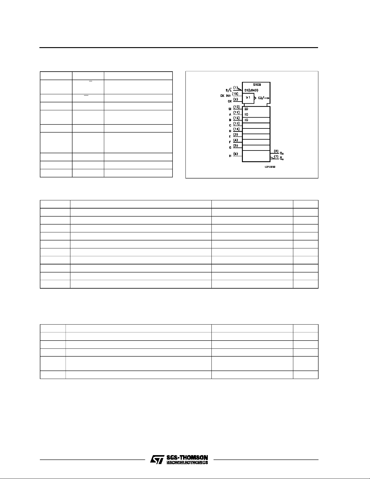
PIN DESCRIPTION
IEC LOGIC SYMBOL
PIN No SYMBOL NAME AND FUNCTION
1 S/L Asynchronous Parallel
Load Input
2 QH Complementary Output
7 QH Serial Output
9 CLOCK Clock Input (LOW to
HIGH edge triggered)
10 SI Serial Data Input
11, 12, 13,
A to H Parallel Data Inputs
14, 3, 4, 5,
6
15 CLOCK INH CLock Inhibit
8 GND Ground (0V)
16 V
CC
Positive Supply Voltage
ABSOLU TE M AXIMU M R AT INGS
Symbol Parameter Value Unit
V
CC
V
V
O
I
IK
I
OK
I
O
or I
I
CC
P
D
T
stg
T
AbsoluteMaximumRatingsarethosevalues beyondwhichdamage tothedevicemayoccur.Functionaloperationunder these conditionisnotimplied.
(*)500 mW: ≅ 65oC derateto300 mWby 10mW/oC: 65oCto85oC
Supply Voltage -0.5 to +7 V
DC Input Voltage -0.5 to VCC+ 0.5 V
I
DC Output Voltage -0.5 to VCC+ 0.5 V
DC Input Diode Current ± 20 mA
DC Output Diode Current ± 20 mA
DC Output Source Sink Current Per Output Pin ± 25 mA
DC VCCor Ground Current ± 50 mA
GND
Power Dissipation 500 (*) mW
Storage Temperature -65 to +150
Lead Temperature (10 sec) 300
L
o
C
o
C
RECO MM ENDED OPERATIN G CO NDI TIONS
Symbol Parameter Value Unit
V
V
T
t
V
r,tf
Supply Voltage 4.5 to 5.5 V
CC
Input Voltage 0 to V
I
Output Voltage 0 to V
O
Operating Temperature: M54HC Series
op
M74HC Series
CC
CC
-55 to +125
-40 to +85
Input Rise and Fall Time (VCC= 4.5 to 5.5V) 0 to 500 ns
V
V
o
C
o
C
3/13
M54/M74HCT165
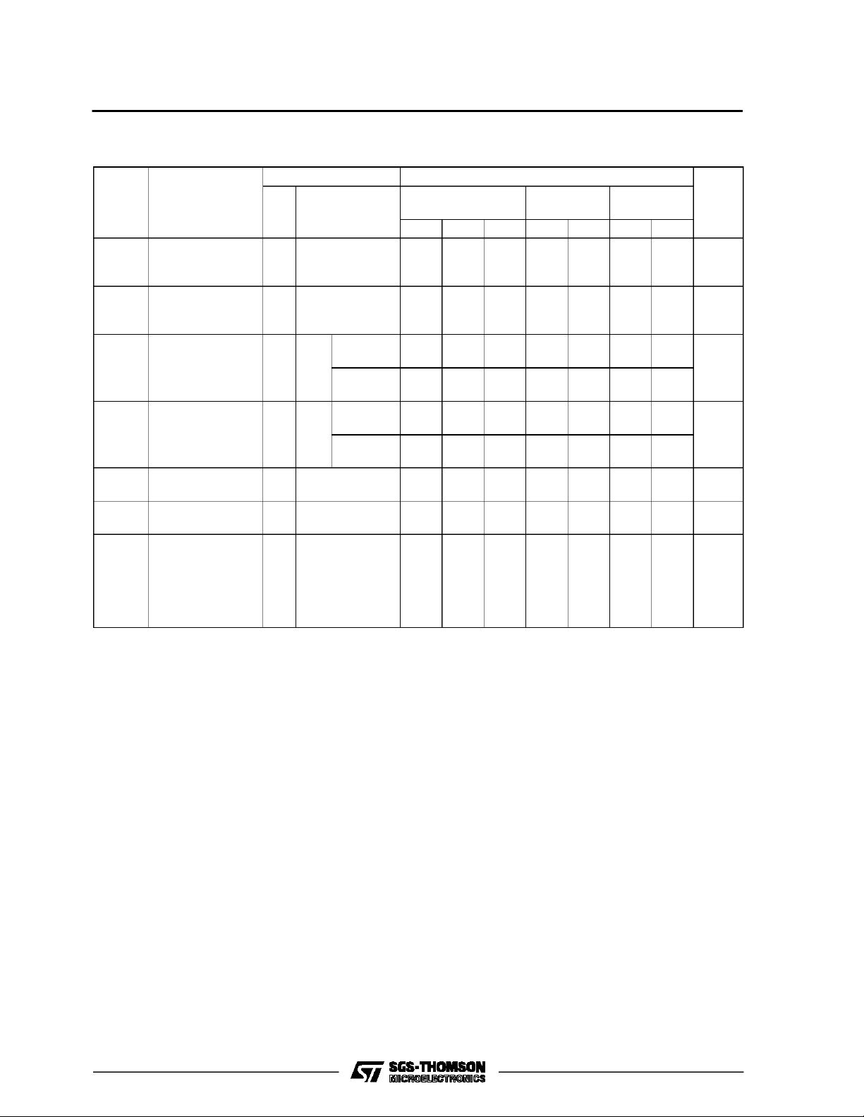
DC SPECIFICATIONS
Symbol Parameter
V
V
V
V
I
∆I
High Level Input
IH
Voltage
Low Level Input
IL
Voltage
High Level
OH
Output Voltage
Low Level Output
OL
Voltage
Input Leakage
I
I
Current
Quiescent Supply
CC
Current
Additional worst
CC
case supply
current
Test Conditions Value
V
(V)
4.5
CC
=25oC
A
54HC and 74HC
Min. Typ. Max. Min. Max. Min. Max.
2.0 2.0 2.0 V
-40 to 85oC
74HC
-55 to 125oC
54HC
Unit
T
to
5.5
4.5
0.8 0.8 0.8 V
to
5.5
VI=
IO=-20 µA 4.4 4.5 4.4 4.4
V
IH
4.5
or
I
=-4.0 mA 4.18 4.31 4.13 4.10
O
V
IL
VI=
IO=20µA 0.0 0.1 0.1 0.1
V
IH
4.5
or
I
= 4.0 mA 0.17 0.26 0.33 0.4
O
V
IL
VI=VCCor GND ±0.1 ±1 ±1 µA
5.5
5.5 VI=VCCor GND 4 40 80 µA
5.5 Per Input pin
2.0 2.9 3.0 mA
VI= 0.5V or
V
= 2.4V
I
Other Inputs at
VCCor GND
IO=0
V
V
4/13
 Loading...