

SGS Thomson Microelectronics M74HCT164 Datasheet
.HIGH SPEED
tPD= 20 ns(TYP.) AT VCC=5V
.LOWPOWER DISSIPATION
ICC=4µA(MAX.) AT TA=25°C
.OUTPUTDRIVE CAPABILITY
10 LSTTLLOADS
.BALANCEDPROPAGATION DELAYS
t
PLH=tPHL
=4 mA (MIN.)
.SYMMETRICALOUTPUT IMPEDANCE
IOL=IOH =4 mA (MIN)
.COMPATIBLE WITHTTL OUTPUTS
VIH= 2V (MIN.) VIL= 0.8V (MAX)
.WIDE OPERATINGVOLTAGE RANGE
VCC(OPR)= 2 V TO6 V
.PIN ANDFUNCTION COMPATIBLE
WITH 54/74LS164
DESCRIPTION
M54HCT164
M74HCT164
8 BITSIPO SHIFT REGISTER
B1R
(PlasticPackage)
M1R
(MicroPackage)
ORDER CODES :
M54HC T164F1R M74H CT164M1R
M74HC T164B1R M74HCT164C1R
F1R
(CeramicPackage)
C1R
(Chip Carrier)
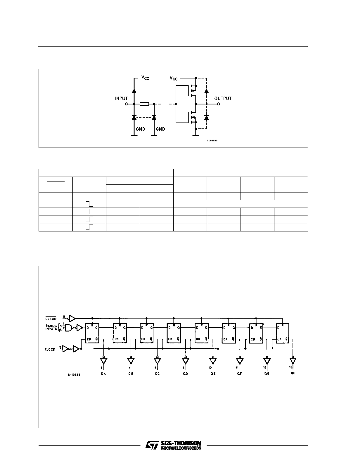
The M54/74HCT164 is a high speed CMOS 8 BIT
SIPO SHIFT REGISTER fabricated in silicon gate
C2MOStechnology.It hasthesamehighspeedperformance of LSTTL combined with trueCMOS low
powerconsumption.
The HCT164is an 8bitshift register with serial data
entry and an outputfrom each of the eight stages.
Data isentered seriallythrough one of two inputs (A
or B),either of theseinputscanbeused asanactive
high enable for data entry through the other input.
An unusedinput must be high, or bothinputs connected together. Each low-to-high transition on the
clock input shifts data one place to the right and
entersintoQA,thelogicNANDofthetwodatainputs
(A • B), the datathat existed before the rising clock
edge. A low level on the clear input overrides all
otherinputsand clearstheregister asynchronously,
forcingall Q outputs low.
All inputs are equipped with protection circuits
against static discharge and transient excess voltage.
This integrated circuit has input and output characteristicsthat arefully compatible with 54/74 LSTTL
logic families. M54/74HCT devices are designed to
directly interface HSC2MOSsystems with TTL and
NMOS components. They are also plugin replacements for LSTTL devices giving a reduction of
powerconsumption.
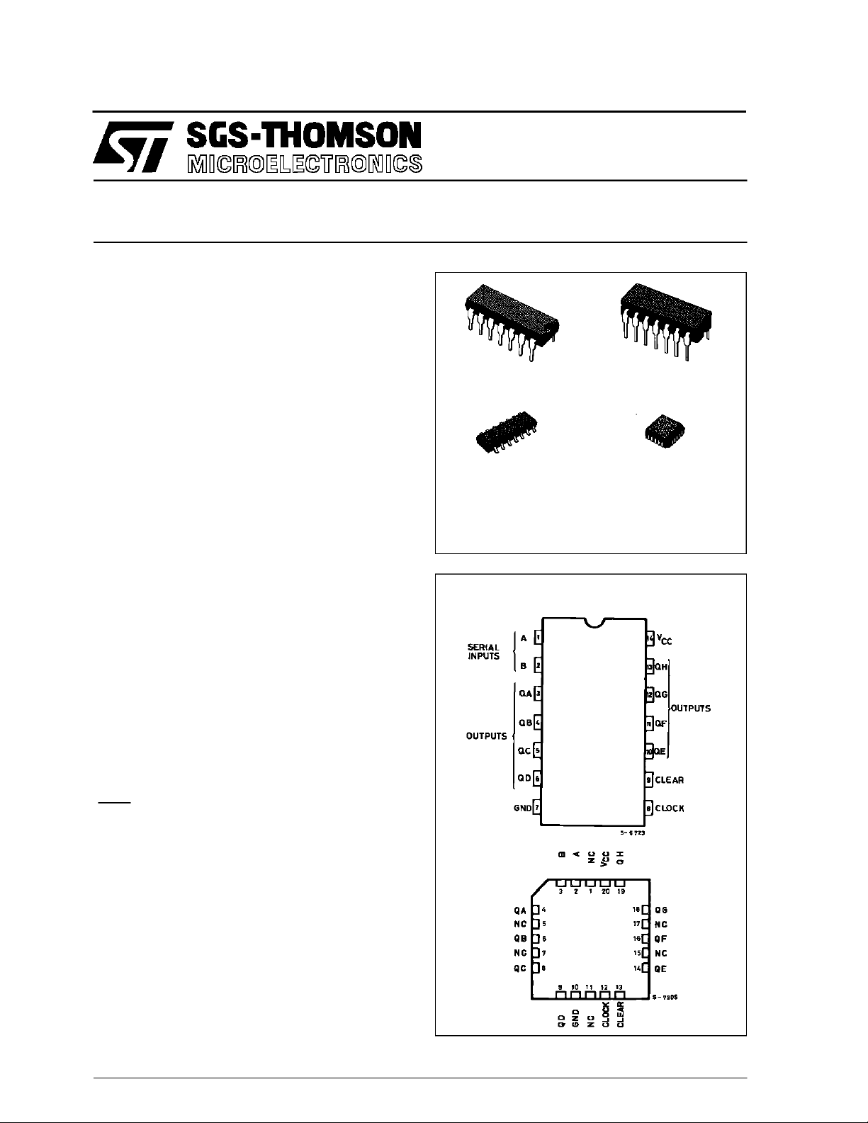
PIN CONNECTIONS(top view)
NC =
No Internal
Connection
February 1993
1/12
M54/M74HCT164
INPUT AND OUTPUT EQUIVALENT CIRCUIT
TRUTH TABLE
INPUTS OUTPUS
CLEAR CLOCK
LXXXLL
H X X NO CHANGE
H L X L QAn
H X L L QAn
H H H H QAn
X:Don’t Care
QAn- QGn : The levelof QA -QG,respectively. before themost-recent transitionof th clock.
SERIAL IN
AB
QA QB ............ QH
............
............
............
............
L
QGn
QGn
QGn
LOGI C DIAG RAM
2/12
M54/M74HCT164
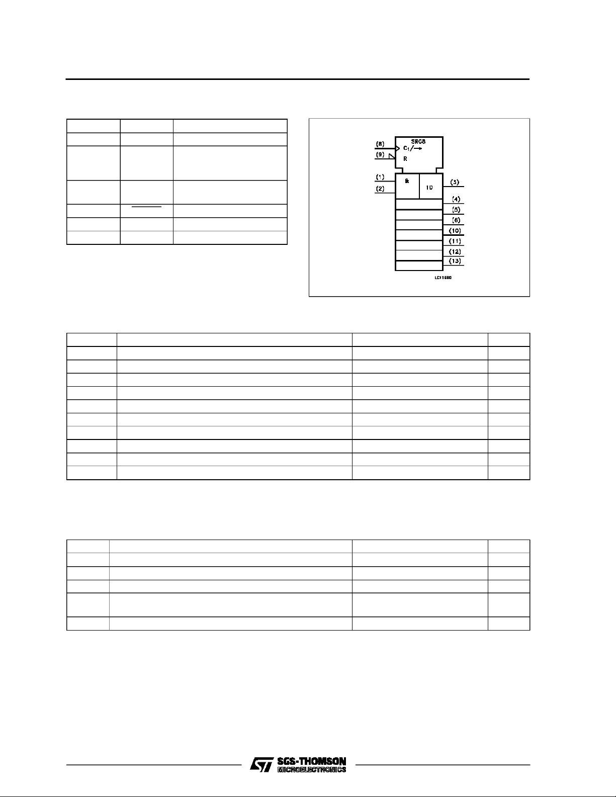
PIN DESCRIPTION
IEC LOGIC SYMBOL
PIN No SYMBOL NAME AND FUNCTION
1, 2 A, B Data Inputs
3, 4, 5, 6,
QA to QH Outputs
10, 11, 12,
13
8 CLOCK Clock Input (LOW to
HIGH, Edge-triggered)
9 CLEAR Master Reset Input
7 GND Ground (0V)
14 V
CC
Positive Supply Voltage
ABSOLU TE MAXIMU M RATINGS
Symbol Parameter Value Unit
V
CC
V
V
O
I
IK
I
OK
I
O
or I
I
CC
P
D
T
stg
T
L
AbsoluteMaximumRatingsarethosevaluesbeyondwhichdamage tothedevicemayoccur.Functionaloperationunder theseconditionisnotimplied.
(*)500 mW:≅ 65oC derateto 300 mWby 10mW/oC: 65oCto85oC
Supply Voltage -0.5 to +7 V
DC Input Voltage -0.5 to VCC+ 0.5 V
I
DC Output Voltage -0.5 to VCC+ 0.5 V
DC Input Diode Current ± 20 mA
DC Output Diode Current ± 20 mA
DC Output Source Sink Current Per Output Pin ± 25 mA
DC VCCor Ground Current ± 50 mA
GND
Power Dissipation 500 (*) mW
Storage Temperature -65 to +150
Lead Temperature (10 sec) 300
o
C
o
C
RECO MM ENDED O PERAT IN G C O NDITI O NS
Symbol Parameter Value Unit
V
V
T
t
V
r,tf
Supply Voltage 4.5 to 5.5 V
CC
Input Voltage 0 to V
I
Output Voltage 0 to V
O
Operating Temperature: M54HC Series
op
M74HC Series
CC
CC
-55 to +125
-40 to +85
Input Rise and Fall Time (VCC= 4.5 to 5.5V) 0 to 500 ns
V
V
o
C
o
C
3/12

M54/M74HCT164
DC SPECIFICATIO NS
Symbol Parameter
V
V
V
V
I
∆I
High Level Input
IH
Voltage
Low Level Input
IL
Voltage
High Level
OH
Output Voltage
Low Level Output
OL
Voltage
Input Leakage
I
I
Current
Quiescent Supply
CC
Current
Additional worst
CC
case supply
current
Test Conditions Value
V
(V)
4.5
CC
=25oC
A
54HC and 74HC
Min. Typ. Max. Min. Max. Min. Max.
2.0 2.0 2.0 V
-40 to 85oC
74HC
-55 to 125oC
54HC
Unit
T
to
5.5
4.5
0.8 0.8 0.8 V
to
5.5
VI=
IO=-20 µA 4.4 4.5 4.4 4.4
V
IH
4.5
or
I
=-4.0 mA 4.18 4.31 4.13 4.10
O
V
IL
VI=
IO=20µA 0.0 0.1 0.1 0.1
V
IH
4.5
or
I
= 4.0 mA 0.17 0.26 0.33 0.4
O
V
IL
VI=VCCor GND ±0.1 ±1 ±1 µA
5.5
5.5 VI=VCCor GND 4 40 80 µA
5.5 Per Input pin
2.0 2.9 3.0 mA
VI= 0.5V or
V
= 2.4V
I
Other Inputs at
VCCor GND
IO=0
V
V
4/12
 Loading...