

SGS Thomson Microelectronics M74HCT14TTR, M74HCT14RM13TR, M74HCT14M1R, M74HCT14B1R Datasheet
M74HCT14
HEX SCHMITT INVERTER
■ HIGH SPEED:
t
= 19ns (TYP.) at VCC = 4.5V
PD
■ LOW POWER DISSIPATION:
= 1µA(MAX.) at TA=25°C
I
CC
■ HIGH NOISE IMMUNITY :
V
= 0.7V (TYP) at Vcc = 4.5V
H
■ BALANCED PROPAGATION DELAYS:
t
≅ t
PLH
■ SYMMETRICAL OUTPUT IMPEDANCE:
|I
OH
■ PIN AND FUNCTION COMPATIBLE WITH
PHL
| = IOL = 4mA (MIN)
74 SERIES 14
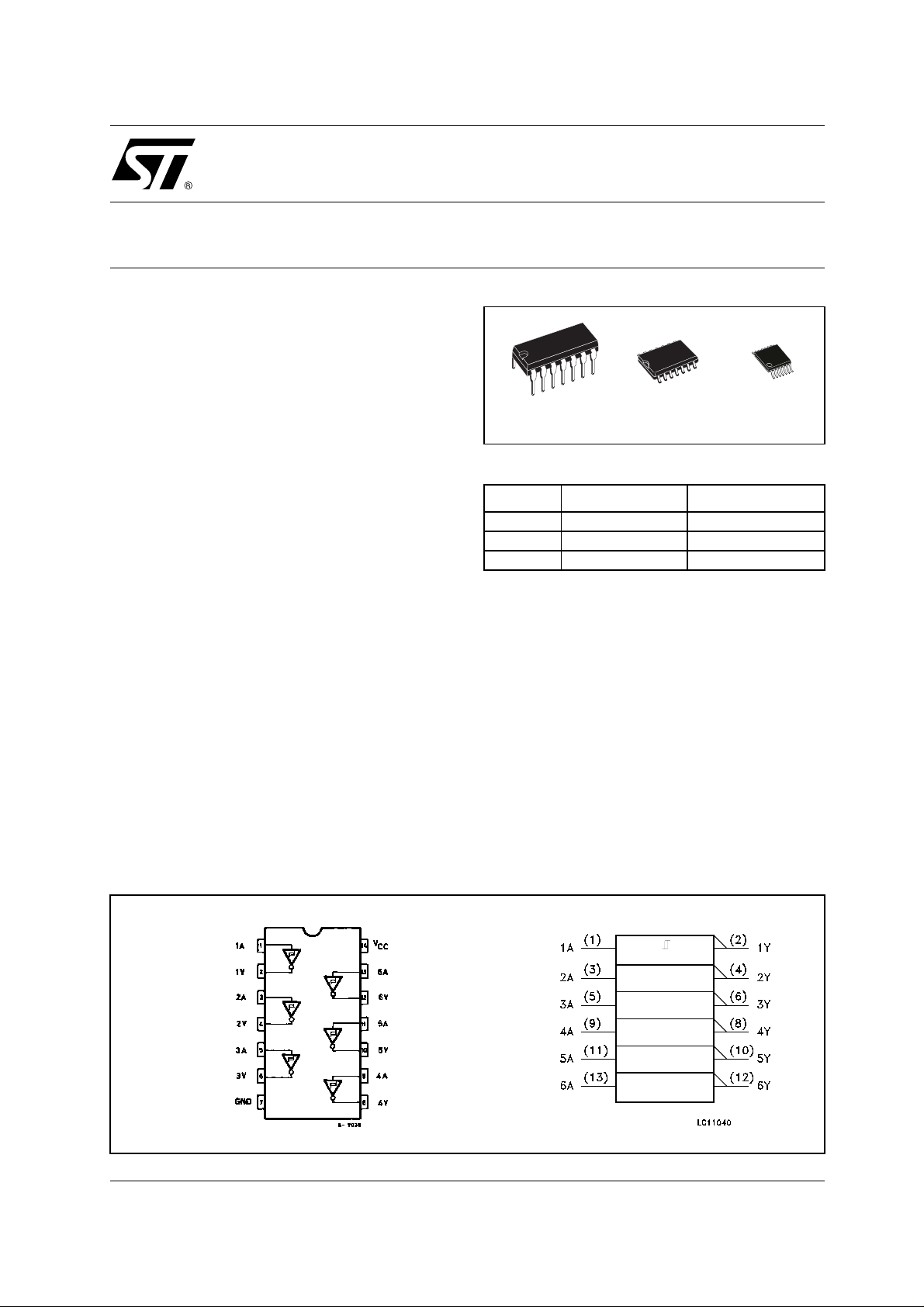
DESCRIPTION
The M74HCT14 is an high speed CMOS HEX
SCHMI TT IN VE RTER fabr icat ed with s ilicon ga te
2
C
MOS technology.
Pin configuration and function are the same as
those of the M74HCT04 but all inputs have 0.7 V
hysteresis level. This together with its schmitt
trigger function allows it to be used on line receiver
with slow rise/fall input signals.
TSSOPDIP SOP
ORDER CODES
PACKAGE TUBE T & R
DIP M74HCT14B1R
SOP M74HCT14M1R M74HCT14RM13TR
TSSOP M74HCT14TTR
The M74HCT14 is designed to directly interface
2
HSC
MOS systems with TTL and NMOS
components.
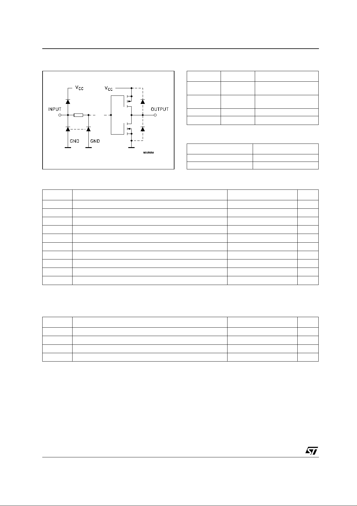
All inputs are equipped with protection circuits
against static discharge and transient excess
voltage.
PIN CONNECTION AND IEC LOGIC SYMBOLS
1/8July 2001
M74HCT14
INPUT AND OUTPUT EQUIVALENT CIRCUIT PIN DESCRIPTION
PIN No SYMBOL NAME AND FUNCTION
1, 3, 5, 9, 1 1,
13
2, 4, 6, 8, 10,
12
7 GND Ground (0V)
14
TRUTH TABLE
ABSOLUTE MAXIMUM RATINGS
Symbol Parameter Value Unit
V
V
V
I
I
OK
I
I
or I
CC
P
T
T
Absolute Maximum Ratings are those values beyond which damage to the device may occur. Functional operation under these conditions is
not implied
(*) 500mW at 65
Supply Voltage
CC
DC Input Voltage -0.5 to VCC + 0.5
I
DC Output Voltage -0.5 to VCC + 0.5
O
DC Input Diode Current
IK
DC Output Diode Current
DC Output Current
O
DC VCC or Ground Current
GND
Power Dissipation
D
Storage Temperature
stg
Lead Temperature (10 sec)
L
°C; derate to 300mW b y 10mW/°C from 65° C to 85°C
1A to 6A Data Inputs
1Y to 6Y Data Outputs
V
CC
Positive Supply Voltage
AY
LH
HL
-0.5 to +7 V
V
V
± 20 mA
± 20 mA
± 25 mA
± 50 mA
500(*) mW
-65 to +150 °C
300 °C
RECOMMENDED OPERATING CONDITIONS
Symbol Parameter Value Unit
V
V
V
T
2/8
Supply Voltage
CC
Input Voltage 0 to V
I
Output Voltage 0 to V
O
Operating Temperature
op
4.5 to 5.5 V
CC
CC
-55 to 125 °C
V
V
DC SPECIFICATIONS
Symbol Param eter
V
High Level
P
Threshold Voltage
V
Low Level
N
Threshold Voltage
V
Hysteresis Voltage 4.5 0.4 0.7 1.4 0.4 1.4 0.4 1.4
H
V
V
I
High Level Output
OH
Voltage
Low Level Output
OL
Voltage
I
Input Leakage
I
Current
Quiescent Supply
CC
Current
M74HCT14
Test Condition Value
T
= 25°C
V
CC
(V)
A
Min. Typ. Max. Min. Max. Min. Max.
4.5 1.2 1.55 1.9 1.2 1.9 1.2 1.9
5.5 1.4 1.75 2.1 1.4 2.1 1.4 2.1
4.5 0.5 0.85 1.2 0.5 1.2 0.5 1.2
5.5 0.6 1.1 1.4 0.6 1.4 0.6 1.4
5.5 0.4 0.7 1.5 0.4 1.5 0.4 1.5
4.5
4.5
5.5
5.5
IO=-20 µA
I
=-4.0 mA
O
IO=20 µA
I
=4.0 mA
O
V
= VCC or GND
I
= VCC or GND
V
I
4.4 4.5 4.4 4.4
4.18 4.31 4.13 4.10
0.0 0.1 0.1 0.1
0.17 0.26 0.33 0.40
-40 to 85°C -55 to 125°C
± 0.1 ± 1 ± 1 µA
11020µA
Unit
V
V
V
V
V
AC ELECTRICAL CHARACTERISTICS (C
= 50 pF, Input tr = tf = 6ns)
L
Test Condition Value
T
Symbol Parameter
t
TLH tTHL
t
PLH tPHL
Output Transition
Time
Propagation Delay
Time
V
CC
(V)
4.5 8151922ns
4.5 19 30 38 45 ns
= 25°C
A
-40 to 85°C -55 to 125°C
Min. Typ. Max. Min. Max. Min. Max.
Unit
CAPACITIVE CHARACTERISTICS
Test Condition Value
T
Symbol Parameter
C
C
Input Capacitance
IN
Power Dissipation
PD
Capacitance (note
V
CC
(V)
= 25°C
A
Min. Typ. Max. Min. Max. Min. Max.
5101010pF
45 pF
1)
1) CPD is defined as the value of the IC’s internal equivalent capacitance which is calculated from the operating current consumption without
load. (R ef er to Test Circuit). Aver age opera ting current can be obta i ned by the following equa tion. I
-40 to 85°C -55 to 125°C
= CPD x VCC x fIN + ICC
CC(opr)
Unit
3/8
 Loading...