

SGS Thomson Microelectronics M74HCT14 Datasheet
.HIGH SPEED
tPD= 16 ns(TYP.) AT VCC=5V
.LOWPOWERDISSIPATION
ICC=1µA(MAX.) AT TA=25°C
.HIGH NOISEIMMUNITY
VH= 0.7 V (TYP.)AT VCC=5V
.OUTPUTDRIVE CAPABILITY
10 LSTTL LOADS
.SYMMETRICALOUTPUT IMPEDANCE
IOH =IOL= 4 mA (MIN.)
.BALANCEDPROPAGATION DELAYS
t
PLH=tPHL
.PIN AND FUNCTION COMPATIBLE WITH
54/74LS14
DESCRIPTION
The M54/74HCT14 is a high speed CMOS HEX
SCHMITT INVERTER fabricated in silicon gate
C2MOStechnology. Ithasthesamehighspeedperformance of LSTTL combined with trueCMOS low
power consumption. Pinconfiguration and function
are the same as those of the HCT04but all inputs
have 0.7 V hysteresis level.This together with its
schmitt trigger functionallows it to be used on line
receivers with slow rise/fall inputsignals. Thisintegrated circuit has input and output characteristics
that are fully compatible with 54/74 LSTTL logic
families. M54/74HCT devices are designed to directly interface HSC2MOS systems with TTL and
NMOS components. They are also plugin replacements for LSTTL devices giving a reduction of
power consumption.All inputs areequipped with pro-
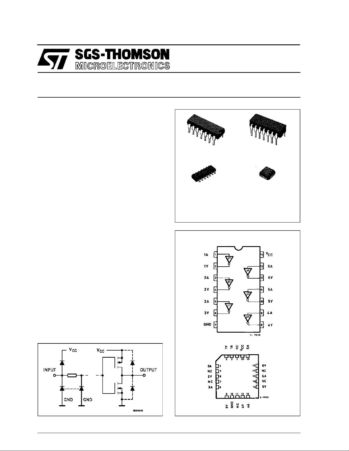
M54HCT14
M74HCT14
HEX SCHMITT INVERTER
B1R
(PlasticPackage)
M1R
(MicroPackage)
ORDER CODES :
M54HC T14F1R M74H CT14M1R
M74HC T14B1R M74HCT14C1R
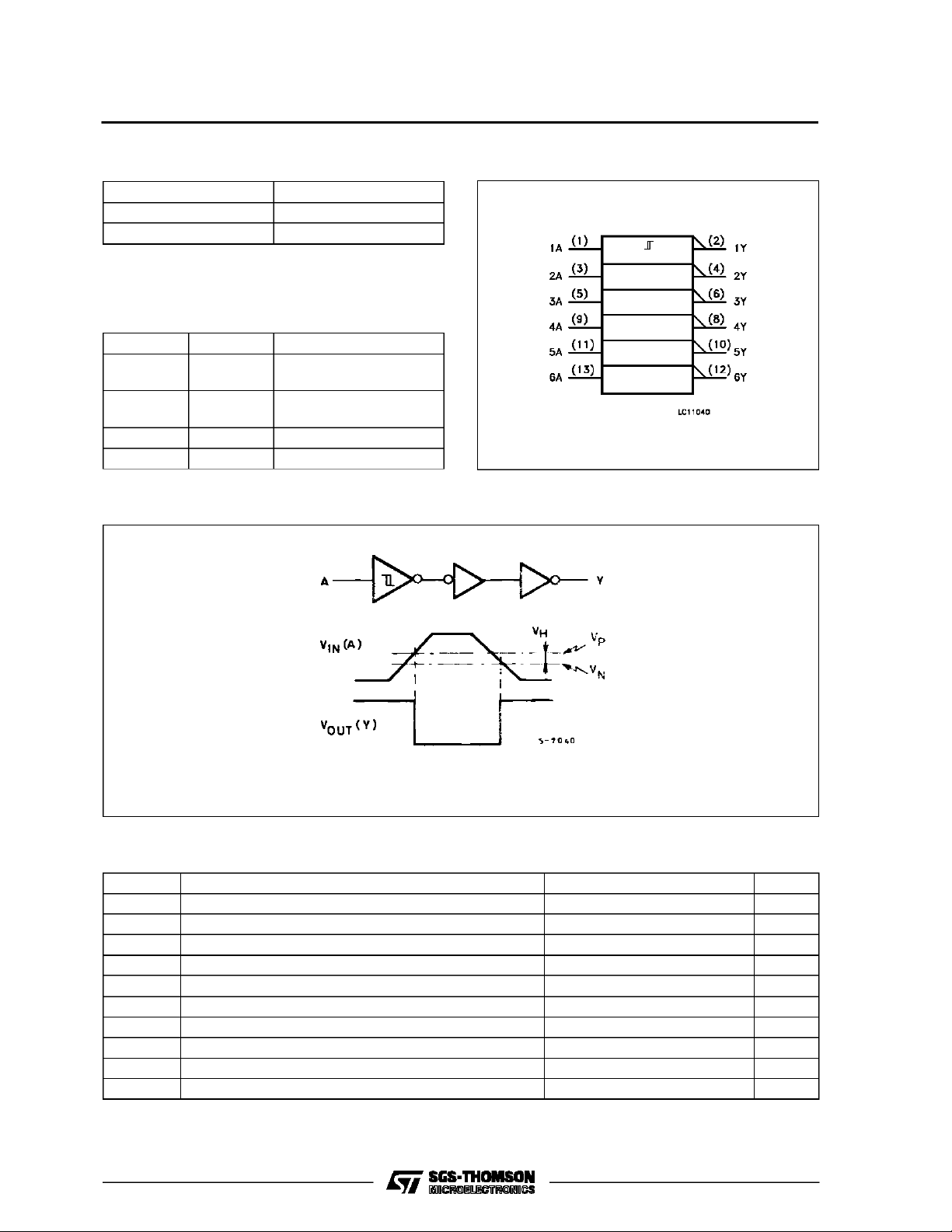
PIN CONNECTIONS(top view)
F1R
(CeramicPackage)
C1R
(Chip Carrier)
INPUT AND OUTPUT EQUIVALENT CIRCUIT
October 1993
NC =
No Internal
Connection
1/9
M54/M74HCT14
TRUTH TABLE
AY
LH
HL
PIN DESCRIPTION
PIN No SYMBOL NAME AND FUNCTION
1, 3, 5, 9,
1A to 6A Data Inputs
11, 13
2, 4, 6, 8,
1Y to 6Y Data Outputs
10,12
7 GND Ground (0V)
14 V
CC
Positive Supply Voltage
LOGI C DI AG RAM /W AVEFORM
IEC LOGIC SYMBOL
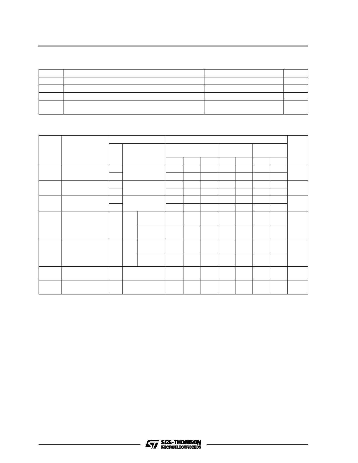
ABSOLU TE MAXI MU M RAT INGS
Symbol Parameter Value Unit
V
CC
V
V
O
I
IK
I
OK
I
O
or I
I
CC
P
D
T
stg
T
L
AbsoluteMaximumRatingsarethose values beyondwhichdamage tothedevicemayoccur. Functionaloperationunder these conditionisnotimplied.
(*)500 mW: ≅ 65oC derateto300mWby 10mW/oC: 65oCto85oC
2/9
Supply Voltage -0.5 to +7 V
DC Input Voltage -0.5 to VCC+ 0.5 V
I
DC Output Voltage -0.5 to VCC+ 0.5 V
DC Input Diode Current ± 20 mA
DC Output Diode Current ± 20 mA
DC Output Source Sink Current Per Output Pin ± 25 mA
DC VCCor Ground Current ± 50 mA
GND
Power Dissipation 500 (*) mW
Storage Temperature -65 to +150
Lead Temperature (10sec) 300
o
C
o
C
M54/M74HCT14
RECO MM ENDED OPERATING CONDI TIONS
Symbol Parameter Value Unit
V
V
V
T
DC SPECIFICATIONS
Symbol Parameter
V
V
V
V
OH
V
OL
I
I
CC
Supply Voltage 4.5 to 5.5 V
CC
Input Voltage 0 to V
I
Output Voltage 0 to V
O
Operating Temperature: M54HC Series
op
M74HC Series
CC
CC
-55 to +125
-40 to +85
Test Conditions Value
T
High Level
P
Threshold Voltage
High Level
N
Threshold Voltage
Hysteresis
H
Voltage
High Level
Output Voltage
Low Level Output
Voltage
Input Leakage
I
Current
Quiescent Supply
=25oC
V
(V)
CC
A
54HC and 74HC
Min. Typ. Max. Min. Max. Min. Max.
4.5 1.2 1.55 1.9 1.2 1.9 1.2 1.9 V
5.5 1.4 1.75 2.1 1.4 2.1 1.4 2.1
4.5 0.5 0.85 1.2 0.5 1.2 0.5 1.2 V
5.5 0.6 1.1 1.4 0.6 1.4 0.6 1.4
4.5 0.4 0.7 1.4 0.4 1.4 0.4 1.4 V
5.5 0.4 0.7 1.5 0.4 1.5 0.4 1.5
VI=
IO=-20 µA 4.4 4.5 4.4 4.4
V
IH
4.5
or
I
=-4.0 mA 4.18 4.31 4.13 4.10
O
V
IL
VI=
IO=20µA 0.0 0.1 0.1 0.1
V
IH
4.5
or
I
= 4.0 mA 0.17 0.26 0.33 0.4
O
V
IL
VI=VCCor GND ±0.1 ±1 ±1 µA
5.5
5.5 VI=VCCor GND 1 10 20 µA
-40 to 85oC
74HC
-55 to 125oC
Current
54HC
V
V
o
C
o
C
Unit
V
V
3/9
 Loading...