

SGS Thomson Microelectronics M74HCT138 Datasheet
3 TO8 LINE DECODER (INVERTING)
.HIGH SPEED
tPD= 16 ns(TYP.) at VCC=5V
.LOWPOWER DISSIPATION
ICC=4µAATTA=25°C
.OUTPUTDRIVE CAPABILITY
10 LSTTLLOADS
.BALANCEDPROPAGATION DELAYS
t
PLH=tPHL
.SYMMETRICALOUTPUT IMPEDANCE
|IOH|=I
OL
.COMPATIBLE WITHTTL OUTPUTS
VIH= 2V (MIN.) VIL= 0.8V (MAX)
.PIN ANDFUNCTION COMPATIBLE
WITH 54/74LS138
DESCRIPTION
The M54/74HC138 is a high speed CMOS 3 TO 8
LINE DECODER fabricated in silicon gate C2MOS
technology. It has the same high speed performanceofLSTTL combinedwithtrueCMOSlowpower
consumption. If the device is enabled, 3 binaryselect inputs(A, Band C)determine whichone ofthe
outputs will go low.If enableinput G1 is held lowor
eitherG2A or G2B is held high, the decoding function is inhibited andall the8 outputs go high. Three
enableinputsare providedtoeasecascadeconnection and application of address decoders for memory systems.Allinputs are equipped with protection
circuitsagainst static discharge and tran- sient excess voltage.This integrated circuit has input and
outputcharacteristics that arefully compatiblewith
54/74 LSTTL logic families. M54/74HCT devices
are designed to directly interface HSC2MOS systems with TTL and NMOS components. They are
also plugin replacements for LSTTL devicesgiving
a reduction of power consumption.
M54HCT138
M74HCT138
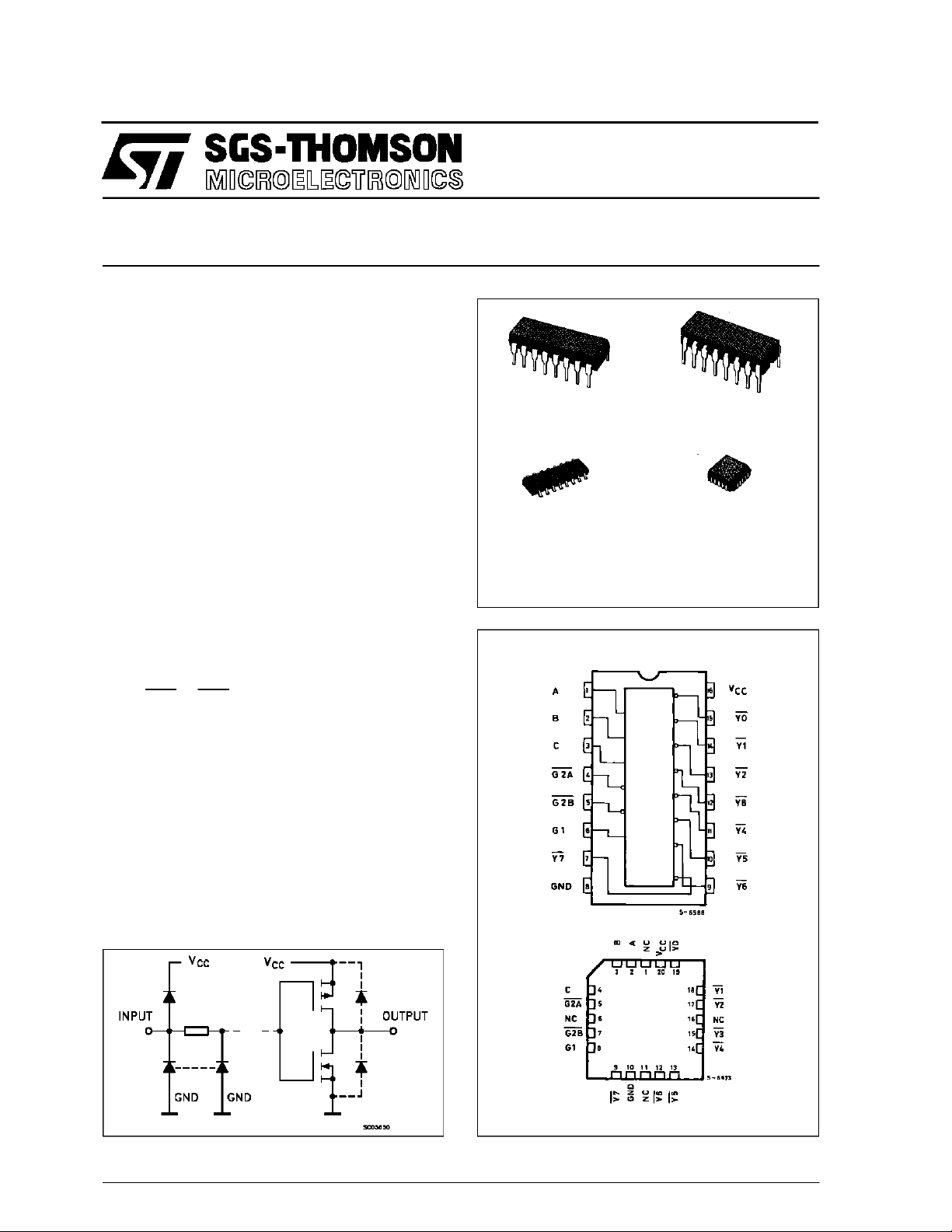
B1R
(PlasticPackage)
M1R
(MicroPackage)
ORDER CODES :
M54HC T138F1R M74H CT138M1R
M74HC T138B 1 R M74HCT 138C1 R
PIN CONNECTIONS(top view)
F1R
(CeramicPackage)
C1R
(Chip Carrier)
INPUT AND OUTPUT EQUIVALENT CIRCUIT
February 1993
NC =
No Internal
Connection
1/10
M54/M74HCT138
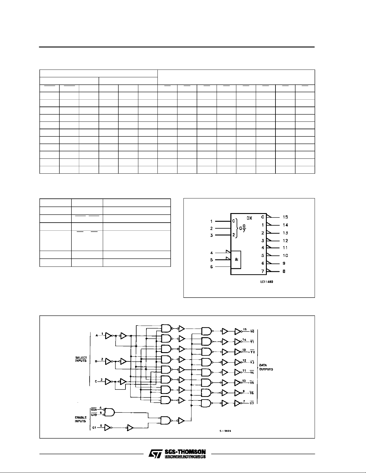
TRUTH TABLE
INPUTS
ENABLE SELECT
G2B G2A G1 C B A Y0 Y1 Y2 Y3 Y4 Y5 Y6 Y7
XXLXXXHHHHHHHH
XHXXXXHHHHHHHH
HXXXXXHHHHHHHH
LLHL L LLHHHHHHH
LLHL LHHLHHHHHH
LLHLHLHHLHHHHH
LLHLHHHHHLHHHH
LLHHL LHHHHLHHH
LLHHLHHHHHHLHH
LLHHHLHHHHHHLH
LLHHHHHHHHHHHL
X:Don’t Care
OUTPUTS
IEC LOGIC SYMBOLPIN DESCRIPTION
PIN No SYMBOL NAME AND FUNCTION
1, 2, 3 A, B, C Address Inputs
4, 5 G2A, G2B Enable Inputs
6 G1 Enable Input
15, 14, 13,
12, 11, 10,
9, 7
8 GND Ground (0V)
16 V
Y0 to Y7 Outputs
CC
Positive Supply Voltage
LOGI C DIAG RAM
2/10
M54/M74HCT138
ABSOLU TE M AXI MU M R AT INGS
Symbol Parameter Value Unit
V
CC
V
V
O
I
IK
I
OK
I
O
I
or I
CC
P
D
T
stg
T
AbsoluteMaximumRatingsarethosevaluesbeyondwhichdamagetothedevice mayoccur. Functionaloperationunder theseconditionisnotimplied.
(*)500 mW:≅ 65oC derateto 300 mWby 10mW/oC: 65oCto85oC
RECO MM ENDED O PERAT IN G CONDI TI O NS
Symbol Parameter Value Unit
V
CC
V
I
V
O
T
op
t
r,tf
Supply Voltage -0.5 to +7 V
DC Input Voltage -0.5 to VCC+ 0.5 V
I
DC Output Voltage -0.5 to VCC+ 0.5 V
DC Input Diode Current ± 20 mA
DC OutputDiode Current ± 20 mA
DC Output Source Sink Current Per Output Pin ± 25 mA
DC VCCor Ground Current ± 50 mA
GND
Power Dissipation 500 (*) mW
Storage Temperature -65 to +150
Lead Temperature (10 sec) 300
L
Supply Voltage 4.5 to 5.5 V
Input Voltage 0 to V
Output Voltage 0 to V
Operating Temperature: M54HC Series
M74HC Series
CC
CC
-55 to +125
-40 to +85
Input Rise and Fall Time (VCC= 4.5 to 5.5V) 0 to 500 ns
o
C
o
C
V
V
o
C
o
C
3/10
 Loading...