

SGS Thomson Microelectronics M74HCT137 Datasheet
3 TO8 LINE DECODER/LATCH (INVERTING)
.HIGH SPEED
tPD= 17 ns(TYP.) AT VCC=5V
.LOWPOWER DISSIPATION
ICC=4µA(MAX.) AT TA=25 °C
.COMPATIBLE WITH TTL OUTPUTS
VIH= 2V (MIN.) VIL= 0.8V (MAX)
.OUTPUT DRIVE CAPABILITY
10 LSTTLLOADS
.SYMMETRICALOUTPUT IMPEDANCE
IOH =IOL= 4 mA(MIN.)
.BALANCEDPROPAGATION DELAYS
t
PLH=tPHL
.PIN ANDFUNCTION COMPATIBLE
WITH 54/74LS137
DESCRIPTION
TheM54/74HCT137isa highspeed CMOS3TO8LINE
DECODE R/ L A TC H (I NVER TI NG) fabri cated in silic o n
gateC2MOStechnol ogy.IthasthesamehighspeedperformanceofLSTTLcombinedwithtrueCMOSlowpower
consumption.Thisdeviceisa 3 to 8 linedecod erwithlatches on the three address inputs. When GL goes from low
tohigh, the addres s presentat theselect input s(A,B and
C) isstored in the latches. Aslong as GLremains high no
addre ss cha nges wi llbe r ecog nized . Outputenable pins
G1an d G2,contro l thestateof theoutputsindependently
oftheselectorlatch-enab le inputs.All theoutputsarehigh
unless G1 is h igh and G2 is low. The HC137 is ideally
suited for the implement ation of glitch -fre e de code rs in
stored-add re ss appl icatio ns in bus orien ted systems.All
inputs are equipped with protectio n ci rcuit s against static
discharge and transien t excess voltage.Thi s integrate d
circuit has input and output characteristics that are fully
compatible with 54/74 LSTTL logic families. M54/74HCT
devicesaredesignedtodirectlyinterfa ceHSC2MOSsystemswithTTLandNMOScomponents.Theyarealso
plugin replacements for LSTTL devices giving a reductionof power consumption.
M54HCT137
M74HCT137
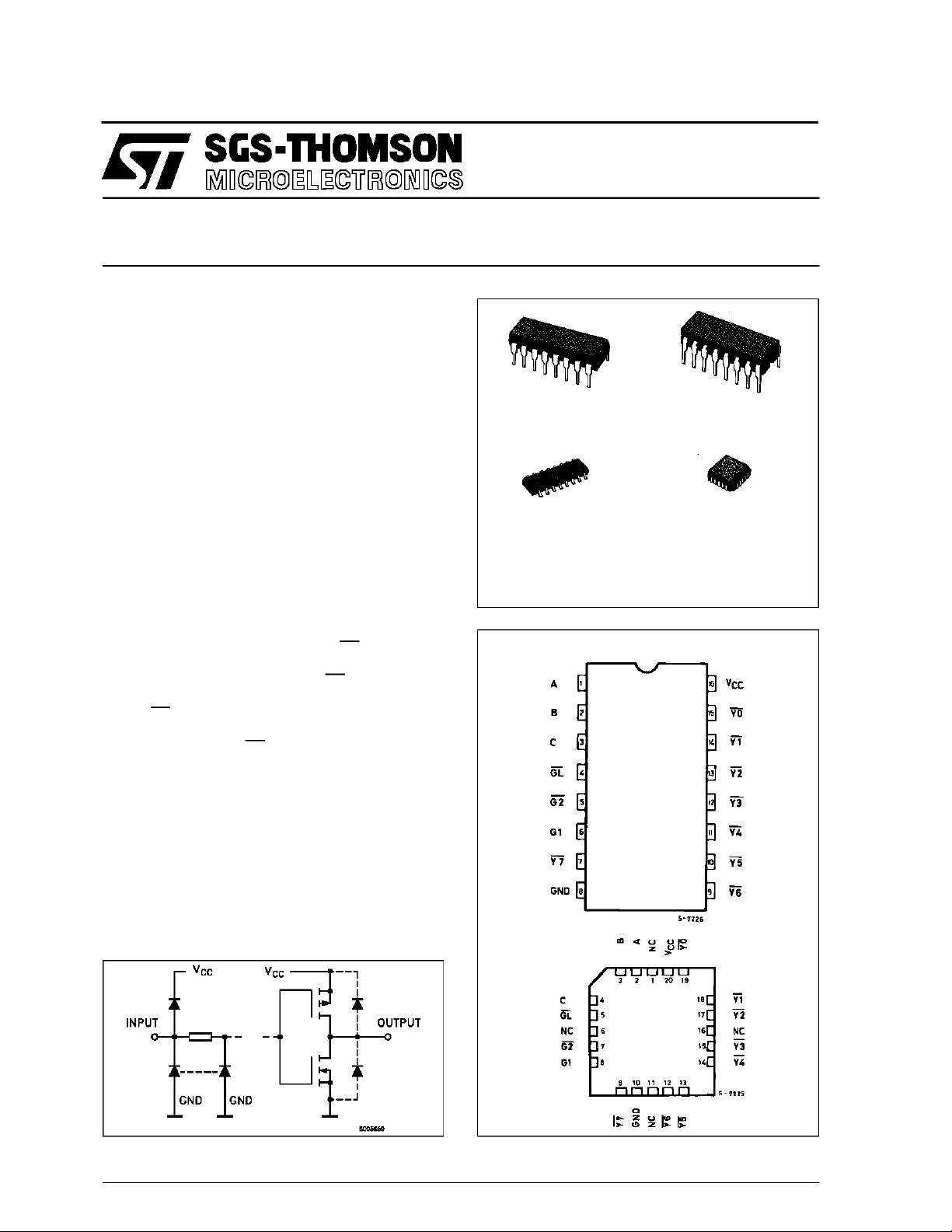
B1R
(PlasticPackage)
M1R
(MicroPackage)
ORDER CODES :
M54HC T137F1R M74H CT137M1R
M74HC T137B1R M74HCT137C1R
PIN CONNECTIONS(top view)
F1R
(CeramicPackage)
C1R
(Chip Carrier)
INPUT AND OUTPUT EQUIVALENT CIRCUIT
February 1993
NC =
No Internal
Connection
1/12
M54/M74HCT137
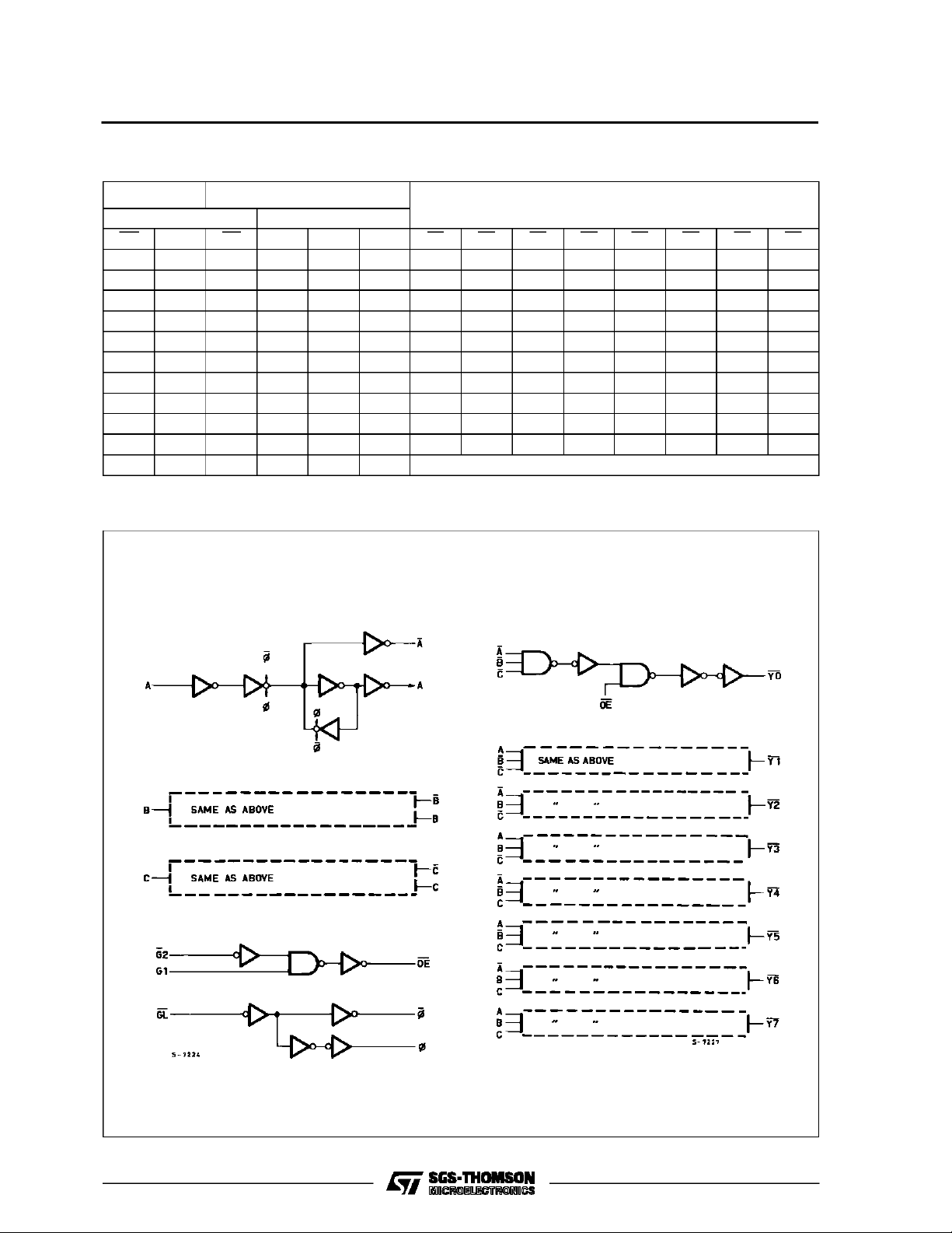
TRUTH TABLE
INPUTS
ENABLE SELECT
GL G1 G2 C B A Y0 Y1 Y2 Y3 Y4 Y5 Y6 Y7
XLXXXXHHHHHHHH
XXHXXXHHHHHHHH
LHL L L LLHHHHHHH
LHL L LHHLHHHHHH
LHL LHLHHLHHHHH
LHL LHHHHHLHHHH
LHLHL LHHHHLHHH
LHLHLHHHHHHLHH
LHLHHLHHHHHHLH
LHLHHHHHHHHHHL
H H L X X X Outputs corresponding to stored address L: all others H
OUTPUTS
LOGI C DIAG RAM
2/12
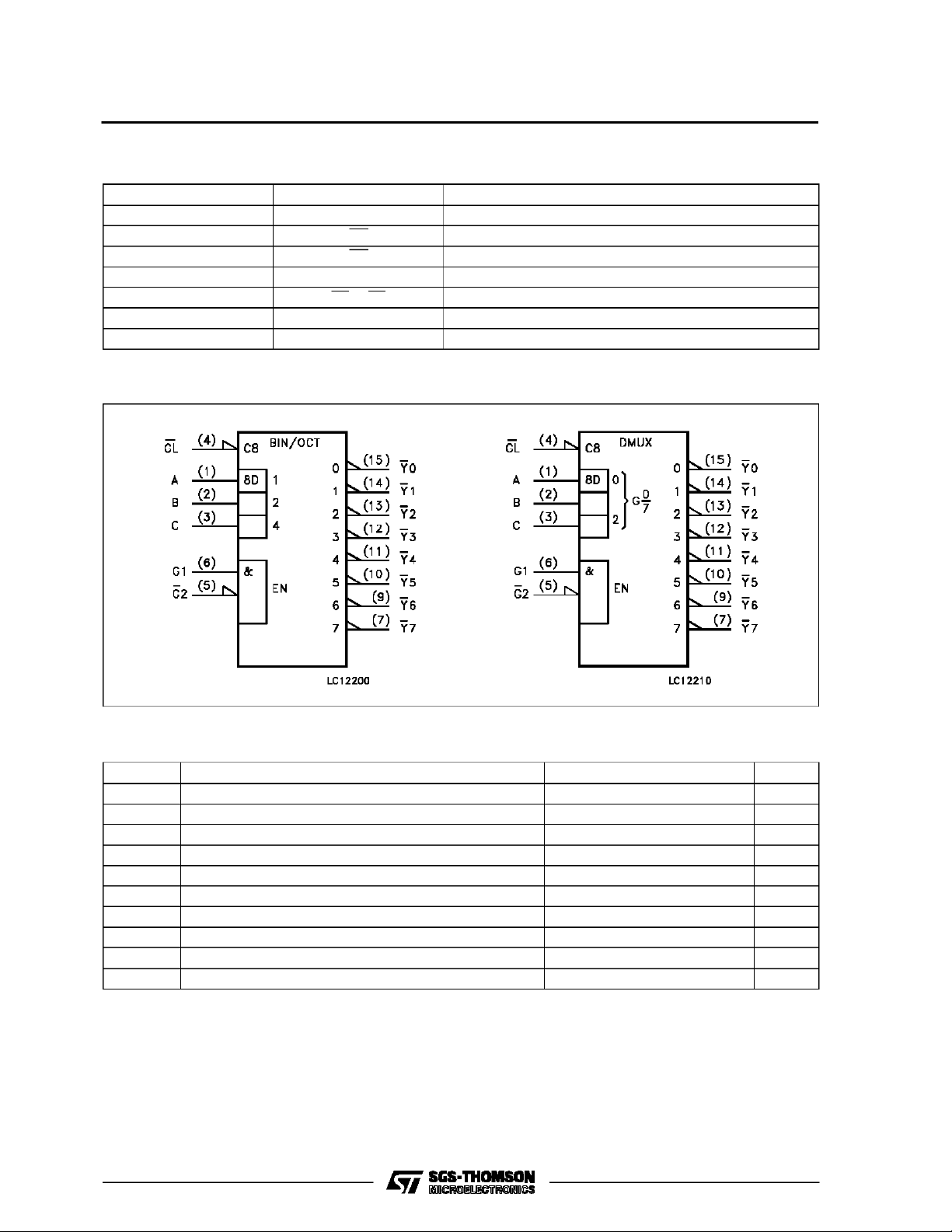
PIN DESCRIPTION
PIN No SYMBOL NAME AND FUNCTION
1, 2, 3 A to C Data Inputs
4 GL Latch Enable Input (Active LOW)
5 G2 Data Enable Input (Active LOW)
6 G1 Data Enable Input (Active HIGH)
15, 14, 13, 12, 11, 10, 9, 7 Y0 to Y7 Multiplexer Outputs
8 GND Ground (0V)
16 V
CC
Positive Supply Voltage
IEC LOGIC SYMBOLS
M54/M74HCT137
ABSOLU TE M AXI MU M R AT INGS
Symbol Parameter Value Unit
V
CC
V
V
O
I
IK
I
OK
I
O
I
or I
CC
P
D
T
stg
T
AbsoluteMaximumRatingsarethosevaluesbeyondwhichdamagetothedevice mayoccur. Functionaloperationunder theseconditionisnotimplied.
(*)500 mW:≅ 65oC derateto 300 mWby 10mW/oC: 65oCto85oC
Supply Voltage -0.5 to +7 V
DC Input Voltage -0.5 to VCC+ 0.5 V
I
DC Output Voltage -0.5 to VCC+ 0.5 V
DC Input Diode Current ± 20 mA
DC OutputDiode Current ± 20 mA
DC Output Source Sink Current Per Output Pin ± 25 mA
DC VCCor Ground Current ± 50 mA
GND
Power Dissipation 500 (*) mW
Storage Temperature -65 to +150
Lead Temperature (10 sec) 300
L
o
C
o
C
3/12
M54/M74HCT137
RECO MM ENDED OPERATI N G CO NDITI O NS
Symbol Parameter Value Unit
V
V
V
T
t
r,tf
DC SPECIFICATIO NS
Symbol Parameter
V
V
V
OH
V
OL
I
I
CC
∆I
Supply Voltage 4.5 to 5.5 V
CC
Input Voltage 0 to V
I
Output Voltage 0 to V
O
Operating Temperature: M54HC Series
op
M74HC Series
CC
CC
-55 to +125
-40 to +85
Input Rise and Fall Time (VCC= 4.5 to 5.5V) 0 to 500 ns
Test Conditions Value
T
High Level Input
IH
Voltage
V
(V)
4.5
=25oC
CC
A
54HC and 74HC
Min. Typ. Max. Min. Max. Min. Max.
2.0 2.0 2.0 V
to
-40 to 85oC
74HC
-55 to 125oC
5.5
Low Level Input
IL
Voltage
4.5
to
0.8 0.8 0.8 V
5.5
High Level
Output Voltage
Low Level Output
Voltage
Input Leakage
I
Current
Quiescent Supply
VI=
IO=-20 µA 4.4 4.5 4.4 4.4
V
IH
4.5
or
I
=-4.0 mA 4.18 4.31 4.13 4.10
O
V
IL
VI=
IO=20µA 0.0 0.1 0.1 0.1
V
IH
4.5
or
I
= 4.0 mA 0.17 0.26 0.33 0.4
O
V
IL
VI=VCCor GND ±0.1 ±1 ±1 µA
5.5
5.5 VI=VCCor GND 4 40 80 µA
Current
Additional worst
CC
case supply
current
5.5 Per Input pin
V
= 0.5V or
I
VI= 2.4V
2.0 2.9 3.0 mA
Other Inputs at
VCCor GND
IO=0
54HC
V
V
o
C
o
C
Unit
V
V
4/12
 Loading...