QUAD 2-INPUT SCHMITT NAND GATE
■ HIGH SPEED: t
■ LOWPOWERDISSIPATION:
I
=1µA (MAX.)at TA=25oC
CC
■ OUTPUT DRIVE CAPABILITY
10LSTTLLOADS
■ HIGH NOISE IMMUNITY
V
(TYP.)= 0.71V AT VCC=4.5V
H
■ SYMMETRICAL OUTPUT IMPEDANCE:
|=IOL=4 mA (MIN)
|I
OH
■ BALANCEDPROPAGATIONDELAYS:
t
≅ t
PLH
PHL
■ PIN AND FUNCTION COMPATIBLE WITH
74SERIES132
DESCRIPTION
The M74HCT132 is a high speed CMOS QUAD
2-INPUT SCHMITT NAND GATE fabricated in
silicon gate C
high speed performanceof LSTTLcombined with
true COMS low power consumption. Pin
= 20 ns (TYP.) at VCC=4.5V
PD
2
MOS tecnology. It has the same
M74HCT132
PRELIMINARY DATA
B1R
(Plastic Package)
ORDERCODES :
M74HCT132B1R M74HCT132M1R
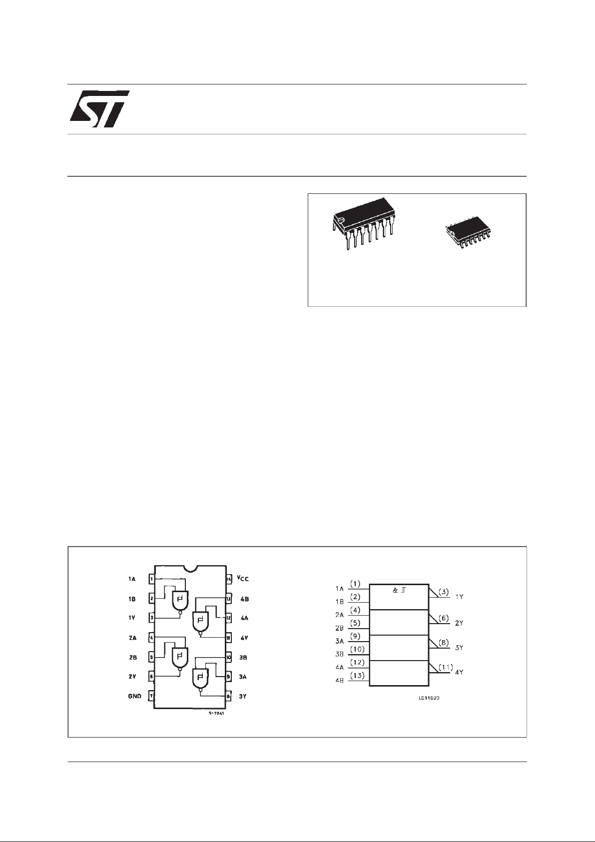
configuration and function are identical to those
of the M74HCT00.
The hysteresis characteristics (around 15% V
of all inputs allow slowly charging input signals to
be transformed into sharply defined jitter-free
output signals.
All inputs are equipped with protection circuits
against static discharge and transient excess
voltage.
M1R
(Micro Package)
CC
)
PINCONNECTION AND IEC LOGIC SYMBOLS
June 1998
1/7

74HCT132
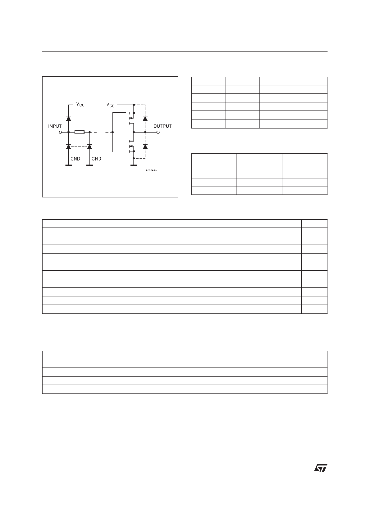
INPUTEQUIVALENT CIRCUIT
PIN DESCRIPTION
PI N No SYM B O L NAME AN D F UNC T I ON
1, 4, 9, 12 1A to 4A Data Inputs
2, 5, 10, 13 1B to 4B Data Inputs
3, 6, 8, 11 1Y to 4Y Data Outputs
7 GND Ground (0V)
14 V
CC
Positive Supply Voltage
TRUTHTABLE
ABY
LLH
LHH
HLH
HHL
ABSOLUTE MAXIMUM RATINGS
Symb o l Parame t er Val u e Uni t
V
V
V
I
I
OK
I
orI
I
CC
P
T
T
Absolute Maximum Ratings are those values beyond which damage to the device may occur. Functional operation under these condition is not implied.
(*)500mW:≅ 65
Supply Voltage -0.5 to +7.0 V
CC
DC Input Voltage -0.5 to VCC+ 0.5 V
I
DC Output Voltage -0.5 to VCC+ 0.5 V
O
DC Input Diode Current ± 20 mA
IK
DC Output Diode Current ± 20 mA
DC Output Current ± 25 mA
O
DC VCCor Ground Current ± 50 mA
GND
Power Dissipation 500 (*) mW
D
Storage Temperature -65 to +150
stg
Lead Temperature (10 sec) 300
L
o
C derate 300 mW by 10 mW/oC: 65oCto80oC
o
C
o
C
RECOMMENDED OPERATINGCONDITIONS
Symb o l Parame t er Value Un i t
V
V
V
T
2/7
Supply Voltage 4.5 to 5.5 V
CC
Input Voltage 0 to V
I
Output Voltage 0 to V
O
Operating Temperature -40 to +85
op
CC
CC
V
V
o
C

DC SPECIFICATIONS
74HCT132
Symbol Parameter Test Conditions Value Unit
T
V
CC
(V)
High Level Threshold
V
t+
Voltage
Low Level Threshold
V
t-
Voltage
Hysteresis Voltage 4.5 0.4 0.7 1.4 0.4 1.4
V
h
4.5 1.2 1.55 1.9 1.2 1.9
5.5 1.4 1.75 2.1 1.4 2.1
4.5 0.5 0.85 1.2 0.5 1.2
5.5 0.6 1.1 1.4 0.6 1.4
Min. Typ. Max. Mi n. M ax.
=25oC-40to85
A
o
C
5.5 0.4 0.7 1.5 0.4 1.5
High Level Output
V
OH
Voltage
V
Low Level Output
OL
Voltage
Input Leakage Current 5.5 VI= 5.5V or GND ±0.1 ±1.0 µA
I
I
Quiescent Supply
I
CC
4.5 V
4.5 I
4.5
4.5 I
5.5 VI=VCCor GND 1 10 µA
(*)
=
IO=-50 µA 4.4 4.5 4.4
I
or
V
IL
V
IH
(*)
V
I
V
IH
=-8 mA 4.18 4.31 4.13
O
IO=50 µA 0.0 0.1 0.1
=
=8 mA 0.17 0.26 0.33
O
Current
(*)All outputs loaded.
AC ELECTRICAL CHARACTERISTICS (CL= 50pF, Input tr=tf=6ns)
Symbol Parameter Test Condition Value Unit
t
Output Transition Time 4.5 7.0 15.0 19.0 ns
TLH
t
THL
t
Propagation Delay
PLH
t
Time
PHL
(*) Voltagerange is3.3V ± 0.3V
(**) Voltagerange is5V ± 0.5V
V
CC
(V)
Min. Typ. Max. Mi n. M ax.
4.5 20.0 33.0 41.0 ns
=25oC-40to85
T
A
o
C
V
V
V
V
V
CAPACITIVE CHARACTERISTICS
Symbol Parameter Test Conditions Value Unit
=25oC-40to85
T
A
Min. Typ. Max. Mi n. M ax.
Input Capacitance 3.5 pF
C
IN
Power Dissipation
C
PD
20 pF
Capacitance (note 1)
1) CPDis defined as the value of the IC’s internal equivalent capacitance which is calculated from the operating current consumption without load. (Refer to
Test Circuit). Average operating current can be obtained by the following equation. I
(opr)= CPD• VCC• fIN+ICC/4(per Gate)
CC
o
C
3/7
 Loading...