

SGS Thomson Microelectronics M74HCT04 Datasheet
.HIGH SPEED
tPD= 8 ns (TYP.) AT VCC=5V
.LOWPOWER DISSIPATION
ICC=1µA(MAX.) AT TA=25°C
.COMPATIBLE WITH TTL OUTPUTS
VIH= 2V (MIN.) VIL= 0.8V(MAX)
.OUTPUT DRIVE CAPABILITY
10 LSTTL LOADS
.SYMMETRICALOUTPUT IMPEDANCE
|IOH|=IOL=4 mA (MIN.)
.BALANCEDPROPAGATION DELAYS
t
PLH=tPHL
.PIN AND FUNCTION COMPATIBLE
WITH 54/74LS04
DESCRIPTION
The M54/74HCT04 is a highspeed CMOS INVERTER fabricated in silicon gate C2MOS technology.
It has the same high speed performance of LSTTL
combined withtrue CMOSlow power consumption.
The internal circuitis composedof 3 stages includingbufferedoutput,whichgiveshighnoiseimmunity
and a stable output.
All inputs are equipped with protection circuits
against staticdischarge or transientexcess voltage.
This integrated circuit has input and outputcharacteristic that are fully compatible with 54/74 LSTTL
logic families. M54HCT/74HCT devices are designedto directly interface HSC2MOSsystems with
TTLand NMOScomponents. They are also plug in
replacements for LSTTL devices giving areduction
of power consumption.
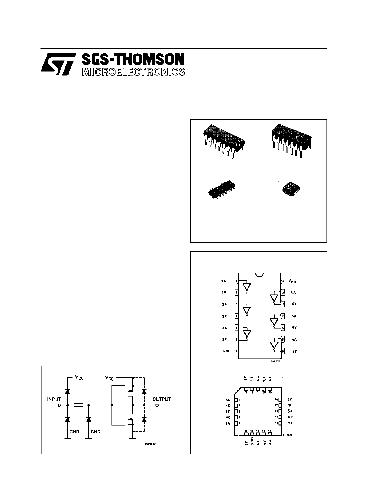
M54HCT04
M74HCT04
HEX INVERTER
B1R
(PlasticPackage)
M1R
(MicroPackage)
ORDER CODES :
M54HC T04F1R M74H CT04M1R
M74HC T04B1R M74HCT04C1R
PIN CONNECTIONS (top view)
F1R
(CeramicPackage)
C1R
(Chip Carrier)
INPUT AND OUTPUT EQUIVALENT CIRCUIT
February 1993
NC =
No Internal
Connection
1/9
M54/M74HCT04
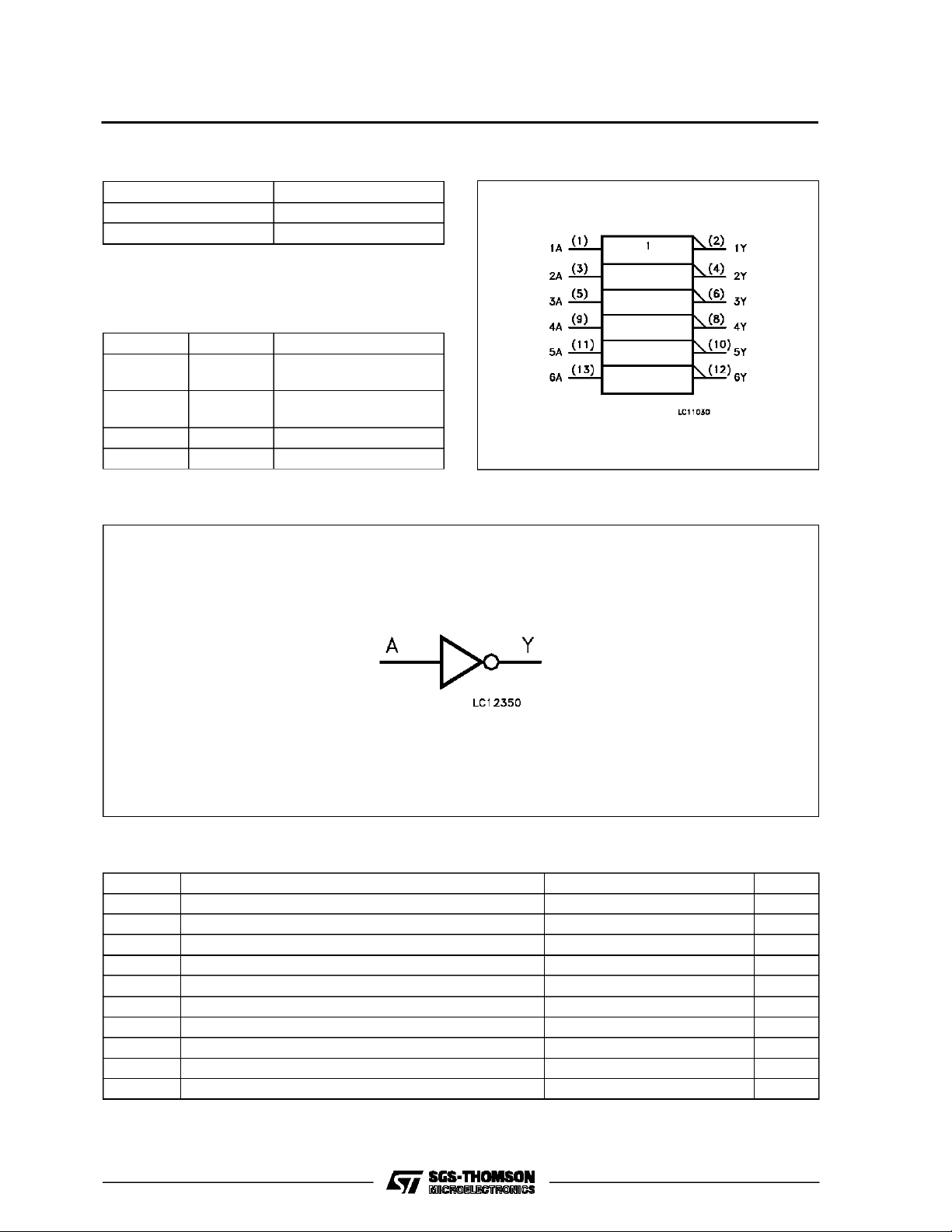
TRUTH TABLE
AY
LH
HL
PIN DESCRIPTION
PIN No SYMBOL NAME AND FUNCTION
1, 3, 5, 9,
1A to 6A Data Inputs
11, 13
2, 4, 6, 8,
1Y to 6Y Data Outputs
10, 12
7 GND Ground (0V)
14 V
CC
Positive Supply Voltage
LOGI C DI AG RAM (Per G at e )
IEC LOGIC SYMBOL
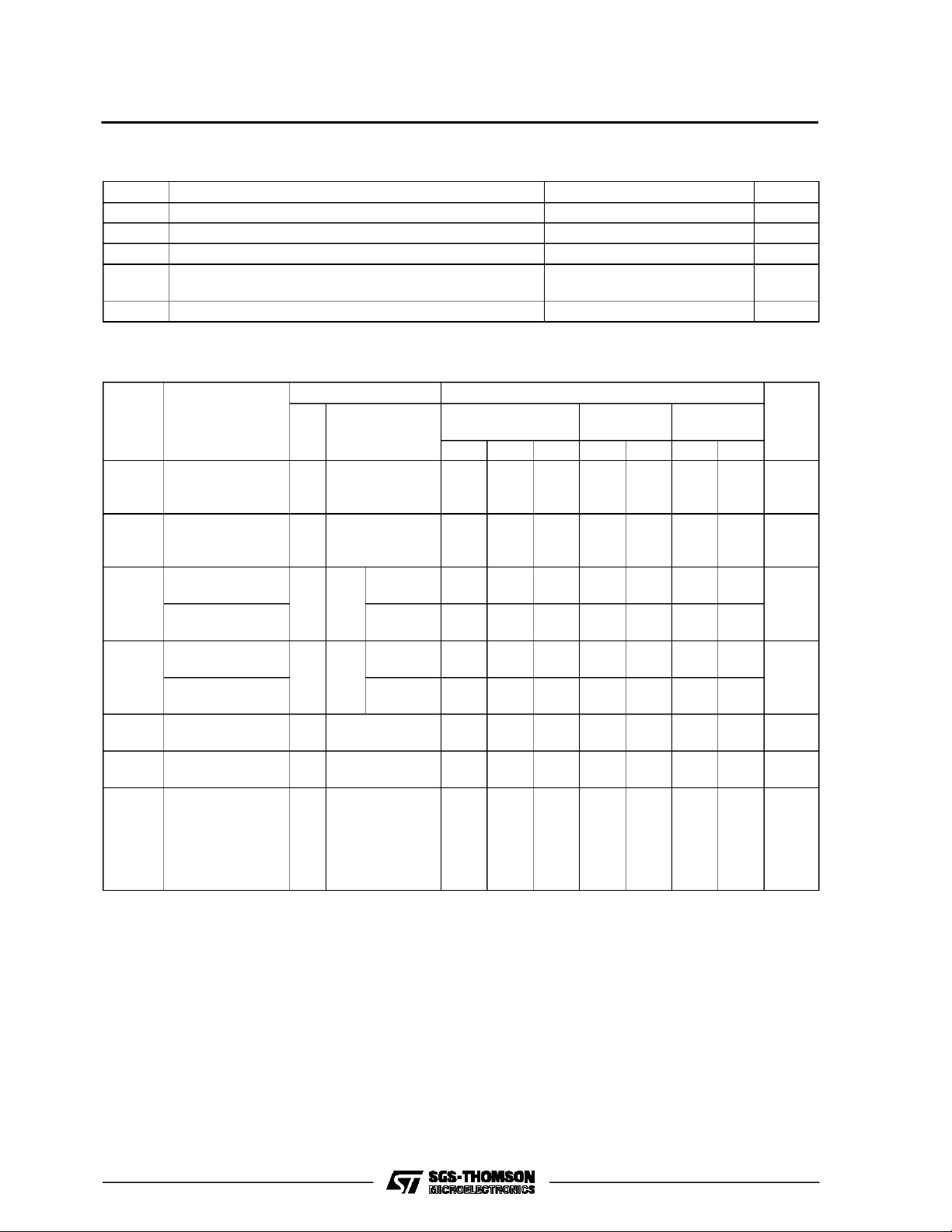
ABSOLU TE MAXI MU M RAT INGS
Symbol Parameter Value Unit
V
CC
V
V
O
I
IK
I
OK
I
O
or I
I
CC
P
D
T
stg
T
L
AbsoluteMaximumRatingsarethosevalues beyond whichdamagetothedevicemayoccur.Functionaloperationunder these conditionisnotimplied.
(*)500 mW:≅ 65oC derateto300mWby 10mW/oC: 65oCto85oC
2/9
Supply Voltage -0.5 to +7 V
DC Input Voltage -0.5 to VCC+ 0.5 V
I
DC Output Voltage -0.5 to VCC+ 0.5 V
DC Input Diode Current ± 20 mA
DC Output Diode Current ± 20 mA
DC Output Source Sink Current Per Output Pin ± 25 mA
DC VCCor Ground Current ± 50 mA
GND
Power Dissipation 500 (*) mW
Storage Temperature -65 to +150
Lead Temperature (10 sec) 300
o
C
o
C
M54/M74HCT04
RECO MM ENDED OPERATI N G C ONDITI ONS
Symbol Parameter Value Unit
V
V
V
T
t
r,tf
DC SPECIFICATIONS
Symbol Parameter
V
V
V
OH
V
OL
I
I
CC
∆I
Supply Voltage 4.5 to 5.5 V
CC
Input Voltage 0 to V
I
Output Voltage 0 to V
O
Operating Temperature: M54HC Series
op
M74HC Series
CC
CC
-55 to +125
-40 to +85
Input Rise and Fall Time (VCC= 4.5 to 5.5V) 0 to 500 ns
Test Conditions Value
T
High Level Input
IH
Voltage
V
(V)
4.5
=25oC
CC
A
54HC and 74HC
Min. Typ. Max. Min. Max. Min. Max.
2.0 2.0 2.0 V
to
-40 to 85oC
74HC
-55 to 125oC
5.5
Low Level Input
IL
Voltage
4.5
to
0.8 0.8 0.8 V
5.5
High Level
Output Voltage
Low Level Output
Voltage
Input Leakage
I
Current
Quiescent Supply
VI=
IO=-20 µA 4.4 4.5 4.4 4.4
V
IH
4.5
or
I
=-4.0 mA 4.18 4.31 4.13 4.10
O
V
IL
VI=
IO=20µA 0.0 0.1 0.1 0.1
V
IH
4.5
or
I
= 4.0 mA 0.17 0.26 0.33 0.4
O
V
IL
VI=VCCor GND ±0.1 ±1 ±1 µA
5.5
5.5 VI=VCCor GND 1 10 20 µA
Current
Additional worst
CC
case supply
current
5.5 Per Input pin
V
= 0.5V or
I
VI= 2.4V
2.0 2.9 3.0 mA
Other Inputs at
VCCor GND
IO=0
54HC
V
V
o
C
o
C
Unit
V
V
3/9
 Loading...