

SGS Thomson Microelectronics M74HC77TTR, M74HC77RM13TR, M74HC77M1R, M74HC77B1R Datasheet
1/10August 2001
■ HIGH SPEED :
t
PD
= 11 ns (TYP.) at VCC = 6V
■ LOW POWER DISSIPATION:
I
CC
=2µA(MAX.) at TA=25°C
■ HIGH NOISE IMMUNITY:
V
NIH
= V
NIL
= 28 % VCC (MIN.)
■ SYMMETRICAL OUTPUT IMPEDANCE:
|I
OH
| = IOL = 4mA (MIN)
■ BALANCED PROPAGATION DELAYS:
t
PLH
≅ t
PHL
■ WIDE OPERATING VOLTAGE RANGE:
V
CC
(OPR) = 2V to 6V
■ PIN AND FUNCTION COMPATIBLE WITH
74 SERIES 77
DESCRIPTION
The M74HC77 is an hi gh speed CMOS 4 BIT D
TYPE LATCH fabricated with silicon gate C
2
MOS
technology.
It contains two groups of 2 bit latches controlled by
an enable input (G1
•2 or G3•4). These two latch
groups can be u sed in different circuit s. The dat a
applied to the d ata inpu ts (1D, 2D, or 3D, 4D) are
transferred to the Q output s (1Q, 2Q, or 3Q , 4Q)
respectively when the enable input (G1
•2 or G3•4)
is taken high. The Q outputs will follow the data
inputs as long as the enable input is kept high.
When the enable input is taken low, the
information data applied to the data input is
retained at the Q outputs.
All inputs are equipped with protection circuits
against static discharge and transient excess
voltage.
M74HC77
4 BIT D TYPE LATCH
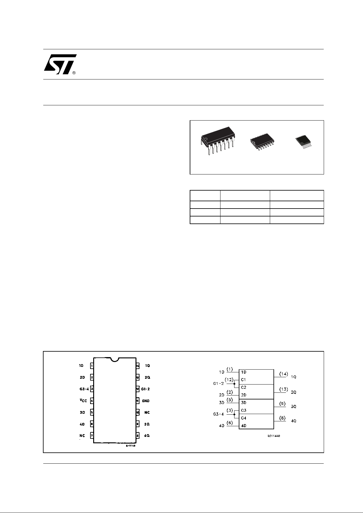
PIN CONNECTION AND IEC LOGIC SYMBOLS
ORDER CODES
PACKAGE TUBE T & R
DIP M74HC77B1R
SOP M74HC77M1R M74HC77RM13TR
TSSOP M74HC77TTR
TSSOPDIP SOP
M74HC77
2/10
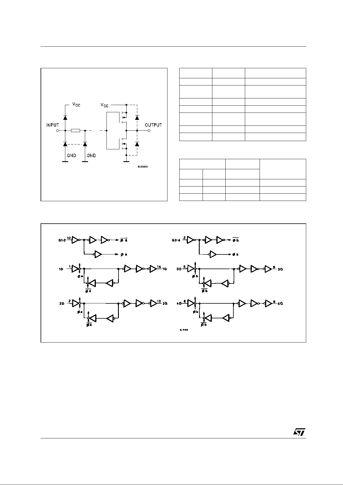
IINPUT AND OUTPUT EQUIVALENT CIRCUIT PIN DESCRIPTION
TRUTH TABLE
X : Don’t Care
LOGIC DIAGRAM
PIN No SYMBOL NAME AND FUNCTION
1, 2, 5, 6 1D to 4D Data Inputs
3G3 • 4
Latch Enable Input,
Latches 3 and 4
7, 10 NC No Internal Connection
8, 9, 13, 14 1Q to 4Q Latch Outputs
12 G1 • 2
Latch Enable Input,
Latches 1 and 2
11 GND Ground (0V)
4
V
CC
Positive Supply Voltage
INPUTS OUTPUTS
FUNCTION
DG Q
LH L
HH H
X L Qn LATCH
M74HC77
3/10
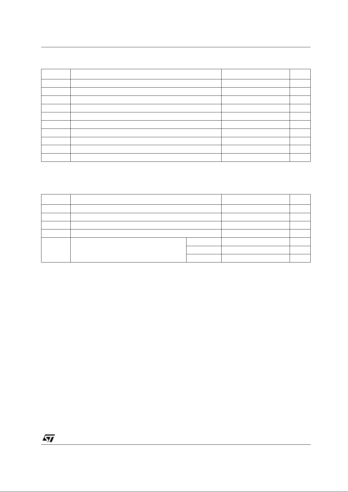
ABSOLUTE MAXIMUM RATINGS
Absolute Maximum Ratings are those values beyond which damage to the device may occur. Functional operation under these conditions is
not implied
(*) 500mW at 65
°C; derate to 300mW by 10mW/°C from 65°C to 85°C
RECOMMENDED OPERATING CONDITIONS
Symbol Parameter Value Unit
V
CC
Supply Voltage
-0.5 to +7 V
V
I
DC Input Voltage -0.5 to VCC + 0.5
V
V
O
DC Output Voltage -0.5 to VCC + 0.5
V
I
IK
DC Input Diode Current
± 20 mA
I
OK
DC Output Diode Current
± 20 mA
I
O
DC Output Current
± 25 mA
I
CC
or I
GND
DC VCC or Ground Current
± 50 mA
P
D
Power Dissipation
500(*) mW
T
stg
Storage Temperature
-65 to +150 °C
T
L
Lead Temperature (10 sec)
300 °C
Symbol Parameter Value Unit
V
CC
Supply Voltage
2 to 6 V
V
I
Input Voltage 0 to V
CC
V
V
O
Output Voltage 0 to V
CC
V
T
op
Operating Temperature
-55 to 125 °C
t
r
, t
f
Input Rise and Fall Time VCC = 2.0V
0 to 1000 ns
V
CC
= 4.5V
0 to 500 ns
V
CC
= 6.0V
0 to 400 ns
 Loading...