

SGS Thomson Microelectronics M74HC77 Datasheet
.HIGH SPEED
tPD= 10 ns(TYP.) AT VCC=5V
.LOWPOWERDISSIPATION
ICC=2µA(MAX.) AT TA=25°C
.HIGH NOISEIMMUNITY
V
NIH=VNIL
=28%VCC(MIN.)
.OUTPUT DRIVE CAPABILITY
10 LSTTL LOADS
.SYMMETRICALOUTPUT IMPEDANCE
IOH =IOL= 4 mA (MIN.)
.BALANCEDPROPAGATION DELAYS
t
PLH=tPHL
.WIDE OPERATINGVOLTAGE RANGE
VCC(OPR)= 2V TO6 V
.PIN AND FUNCTION COMPATIBLE WITH
54/74LS77
DESCRIPTION
The M54/74HC77 is a high speed CMOS 4-BIT DTYPELATCHfabricated in silicongateC2MOStechnology. It has the samehigh speed performance of
LSTTL combined with true CMOS low power consumption.It contains twogroups of 2-bit latches controlled by an enable input (G1• 2orG3•4). These
twolatch groups canbeusedindifferent circuits.The
dataapplied tothedata inputs(1D,2D,or3D,4D)are
transfered to the Q outputs (1Q,2Q, or 3Q, 4Q) respectively whentheenable input(G1 • 2orG3•4) is
takenhigh. The Q outputs will follow thedata inputs
aslong astheenableinputiskepthigh.Whenthe enableinput istaken low, theinformation dataapplied to
thedatainputs is retainedat theQ outputs. All inputs
areequipped withprotectioncircuitsagainst staticdischarge andtransient excess voltage.
M54HC77
M74HC77
4-BIT D-TYPE LATCH
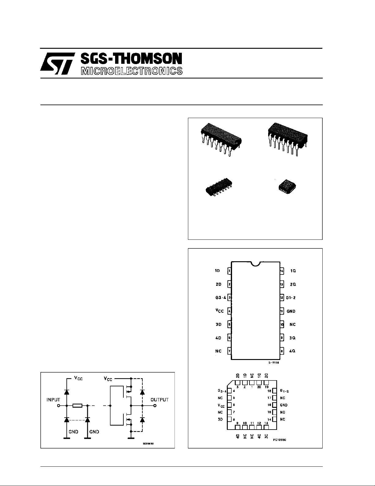
B1R
(PlasticPackage)
M1R
(MicroPackage)
ORDER CODES :
M54HC 77F1R M74H C77M1R
M74HC 77B1R M74HC7 7C1R
PIN CONNECTIONS(top view)
(CeramicPackage)
(Chip Carrier)
F1R
C1R
INPUT AND OUTPUT EQUIVALENT CIRCUIT
October 1992
NC =
No Internal
Connection
1/10
M54/M74HC77
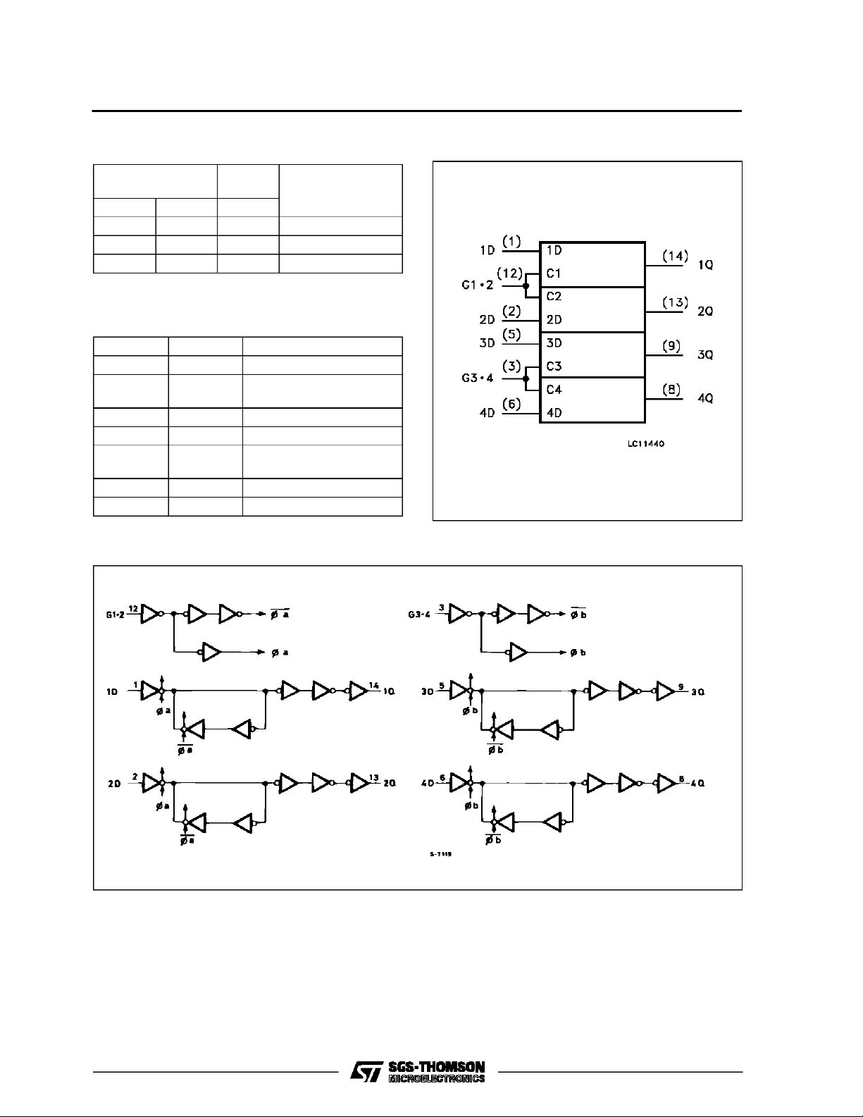
IEC LOGIC SYMBOLTRUTH TABLE
INPUTS
DGQ
LHL
HHH
XLQ
X:Don’t Care
OUTPUTS
n
FUNCTION
LATCH
PIN DESC RIPTION
PIN No SYMBOL NAME AND FUNCTION
1, 2, 5, 6 1D to 4D Data Inputs
3G3•4 Latch Enable Input,
Latches 3 and 4
7, 10 NC No Internal Connection
8, 9, 13, 14 1Q to 4Q Latch Outputs
12 G1 • 2 Latch Enable Input,
Latches 1 and 2
11 GND Ground (0V)
4V
CC
Positive Supply Voltage
LOGI C DI AGRAM
2/10
M54/M74HC77
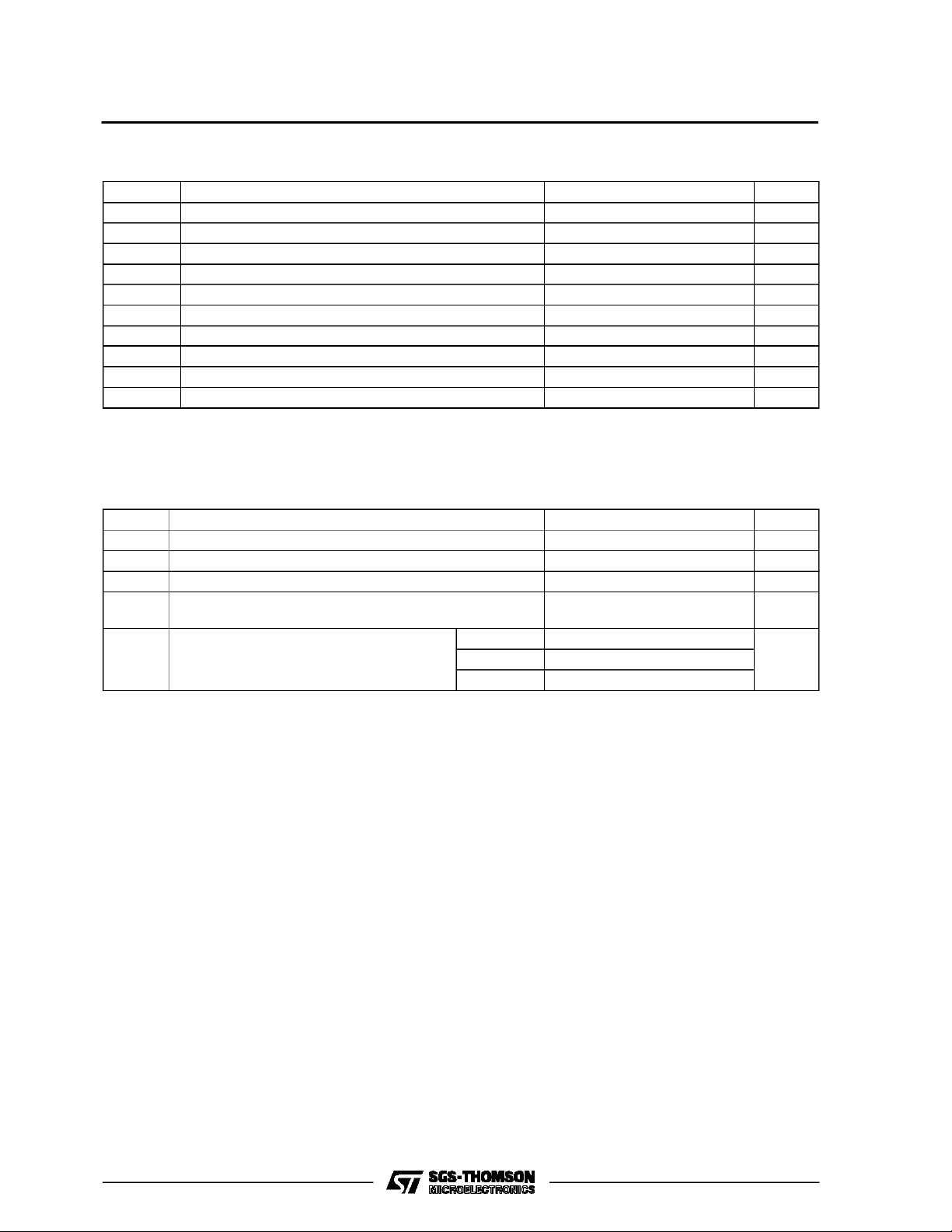
ABSOLU TE M AXIMU M R AT INGS
Symbol Parameter Value Unit
V
CC
V
V
O
I
IK
I
OK
I
O
I
or I
CC
P
D
T
stg
T
AbsoluteMaximumRatingsarethose valuesbeyond whichdamage to thedevice mayoccur.Functional operation under these conditionisnotimplied.
(*)500 mW: ≅ 65oC derateto300 mWby 10mW/oC: 65oCto85oC
RECO MM ENDED OPERATI N G CO NDI TI O NS
Symbol Parameter Value Unit
V
CC
V
I
V
O
T
op
t
r,tf
Supply Voltage -0.5 to +7 V
DC Input Voltage -0.5 to VCC+ 0.5 V
I
DC Output Voltage -0.5 to VCC+ 0.5 V
DC Input Diode Current ± 20 mA
DC Output Diode Current ± 20 mA
DC Output Source Sink Current Per Output Pin ± 25 mA
DC VCCor Ground Current ± 50 mA
GND
Power Dissipation 500 (*) mW
Storage Temperature -65 to +150
Lead Temperature (10sec) 300
L
Supply Voltage 2 to 6 V
Input Voltage 0 to V
Output Voltage 0 to V
Operating Temperature: M54HC Series
M74HC Series
CC
CC
-55 to +125
-40 to +85
Input Rise and Fall Time VCC= 2 V 0 to 1000 ns
V
= 4.5 V 0 to 500
CC
V
= 6 V 0 to 400
CC
o
C
o
C
V
V
o
C
o
C
3/10
 Loading...