

SGS Thomson Microelectronics M74HC7245, M74HC7645, M74HC7640 Datasheet
M54H C 7245/ 764 0/ 7643/ 76 45
M74HC 7 245/ 7640/ 76 43/ 7645
OCTAL BUS TRAN SCEIVER(3-STATE):HC7645NONINVER TING
HC7640 INVERTING ,HC7643 INVERTING/NON INVERTING
.HIGH SPEED
tPD= 12 ns(TYP.) at VCC=5V
.LOWPOWER DISSIPATION
ICC=4µA (MAX.) at TA=25oC
.HIGH NOISE IMMUNITY
VH= 1.1 (TYP.) at VCC=5V
.OUTPUTDRIVE CAPABILITY
15 LSTTLLOADS
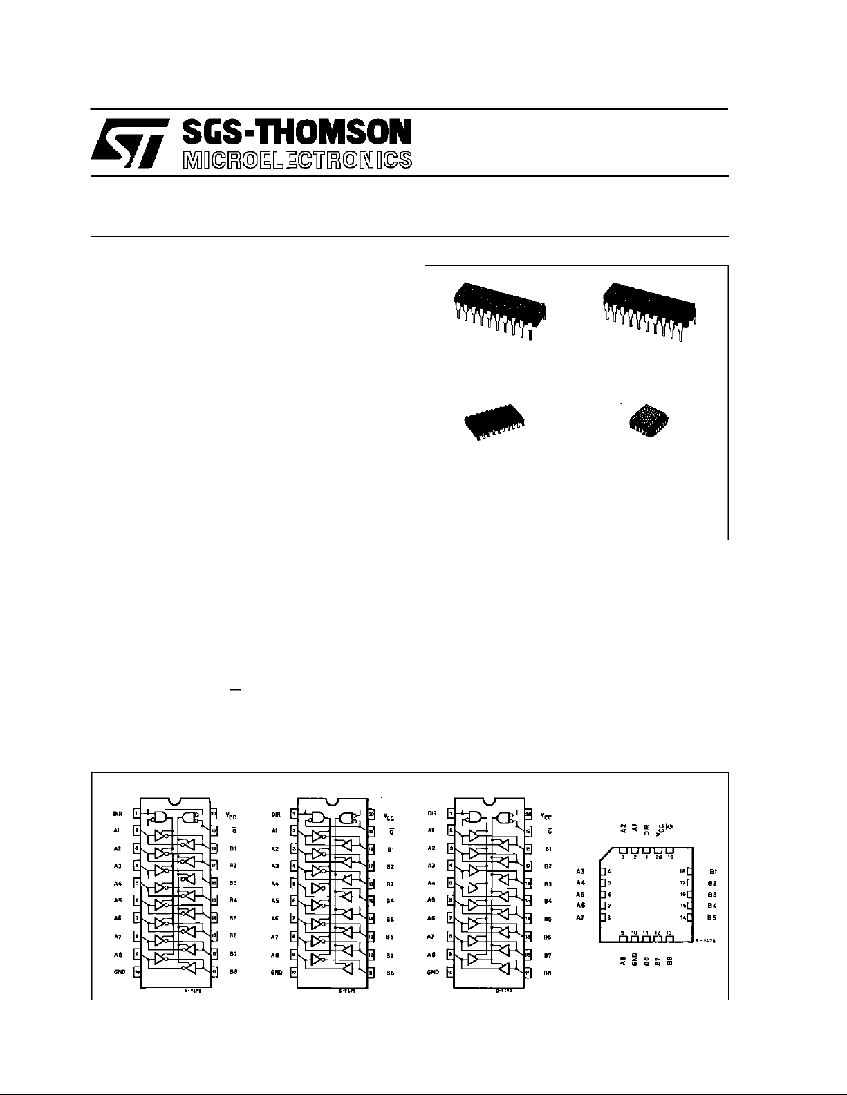
B1R
(PlasticPackage)
F1R
(CeramicPackage)
.SYMMETRICAL OUTPUT IMPEDANCE
|IOH|=IOL=6 mA (MIN)
.BALANCEDPROPAGATIONDELAYS
t
PLH=tPHL
.WIDE OPERATINGRANGE
VCC(OPR)= 2V to 6V
.PIN ANDFUNCTION COMPATIBLE
WITH 54/74LS245/640/643
DESCRIPTION
TheM54/74HC7245 HC7640,HC7643 andHC7645
utilise silicon gate C2MOS technology to achive
operating speeds equivalent to LSTTL devices.
Along withthe low power dissipationand high noise
immunity of standads C2MOS integrated circuit, it
possesses the capability to drive 15 LSTTL loads.
TheseIC’s are intended for two-way asynchronous
communication between data buses, and the
direction of data trasmission is determined by DIR
input.Theenableinput(G)canbeusedtodisablethe
device sothat the buses are effectivelyisolated.
The HC7245/640/7643/7645 have the same pin
configuration and function as the HC245/640/643
andtheyhave a hysteresischaracteristicswith each
input, so HC7245/7640/7643/7645 can be usedas a
line receiver, etc. All input are equipped with
protection circuits against static discharge and
transient excess voltage.
ITISPROHIBITEDTOAPPLYA SIGNALTOA BUS
TERMINAL WHEN IT IS IN OUTPUT MODE AND
WHEN A BUS THERMINAL IS FLOATING (HIGH
IMPEDANCE STATE), IT IS REQUESTED TO FIX
THE INPUT LEVEL BY MEANS OF EXTERNAL
PULLDOWNORPULL UPRESISTOR.
M1R
(MicroPackage)
ORDER CODES :
M54HC XXXXF 1 R M74H CX XXXM1 R
M74HC XXXXB1R M74HCXXXXC1 R
C1R
(Chip Carrier)
PIN CONNECTION (top view)
HC7 640 HC7 643 HC7645/HC7245
HC7245 iselectricallyand funcutionally the same as theHC7645
January 1994
1/10
M54/M74HC7245/7640/7643/7645
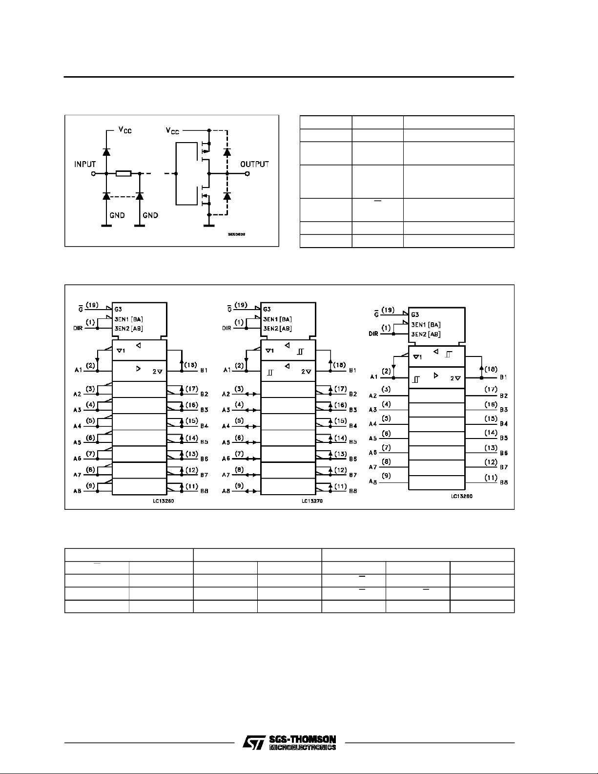
INPUT AND OUTPUT EQUIVALENT CIRCUIT PIN DESCRIPTION
PIN No SYMBOL NAME AND FUNCTION
1 DIR Directional Control
2, 3, 4, 5,
6, 7, 8, 9
18, 17, 16,
15, 14, 13,
12, 11
19 G Output Enabel Input
10 GND Ground (0V)
20 V
IEC LOGIC SYMBOLS
HC7640 HC764 3 HC7645
A1 to A8 Data Inputs/Outputs
B1 to B8 Data Inputs/Outputs
CC
(Active LOW)
Positive Supply Voltage
TRUTH TABLE
INPUT FUNCTION OUTPUT
G DIR A BUS B BUS HC7640 HC7643 HC7645/7245
L L OUTPUT INPUT A = B A = B A = B
L H INPUT OUTPUT B = A B = A B = A
HXZZZZZ
X: ”H” or ”L”
Z: Highimpedance
2/10
M54/M74HC7245/7640/7643/7645
ABSOLU TE M AXI MUM R AT I NG S
Symbol Parameter Value Unit
V
CC
V
V
O
I
IK
I
OK
I
O
I
or I
CC
P
D
T
stg
T
AbsoluteMaximumRatingsarethosevaluesbeyond whichdamagetothedevicemayoccur.Functional operationunder theseconditionisnotimplied.
(*)500 mW:≅ 65oC derate to300 mWby 10mW/oC: 65oCto85oC
RECO MM ENDED OPE RAT IN G CO NDITIO NS
Symbol Parameter Value Unit
V
CC
V
I
V
O
T
op
Supply Voltage -0.5 to +7 V
DC Input Voltage -0.5 to VCC+ 0.5 V
I
DC Output Voltage -0.5 to VCC+ 0.5 V
DC Input Diode Current ± 20 mA
DC Output Diode Current ± 20 mA
DC Output Source Sink Current Per Output Pin ± 35 mA
DC VCCor Ground Current ± 70 mA
GND
Power Dissipation 500 (*) mW
Storage Temperature -65 to +150
Lead Temperature (10 sec) 300
L
Supply Voltage 2 to 6 V
Input Voltage 0 to V
Output Voltage 0 to V
Operating Temperature: M54HC Series
M74HC Series
CC
CC
-55 to +125
-40 to +85
o
C
o
C
V
V
o
C
o
C
3/10
 Loading...