

SGS Thomson Microelectronics M74HC699, M74HC698, M74HC697, M74HC696 Datasheet
M54/74HC696/697
M54/74HC698/699
HC696/698 U/D DEC ADE COUNTER/ REGISTER (3-STATE)
HC697/699 U/D 4 BIT BINARY COU NTER/REG ISTER (3-STATE)
.HIGH SPEED
f
= 50 MHz (TYP.) AT VCC=5V
MAX
.LOWPOWER DISSIPATION
ICC=4µA(MAX.) AT TA=25°C
.HIGH NOISE IMMUNITY
V
NIH=VNIL
.OUTPUT DRIVE CAPABILITY
15 LSTTL LOADS (for QAto QD)
10 LSTTL LOADS (for RCO)
=28%VCC(MIN.)
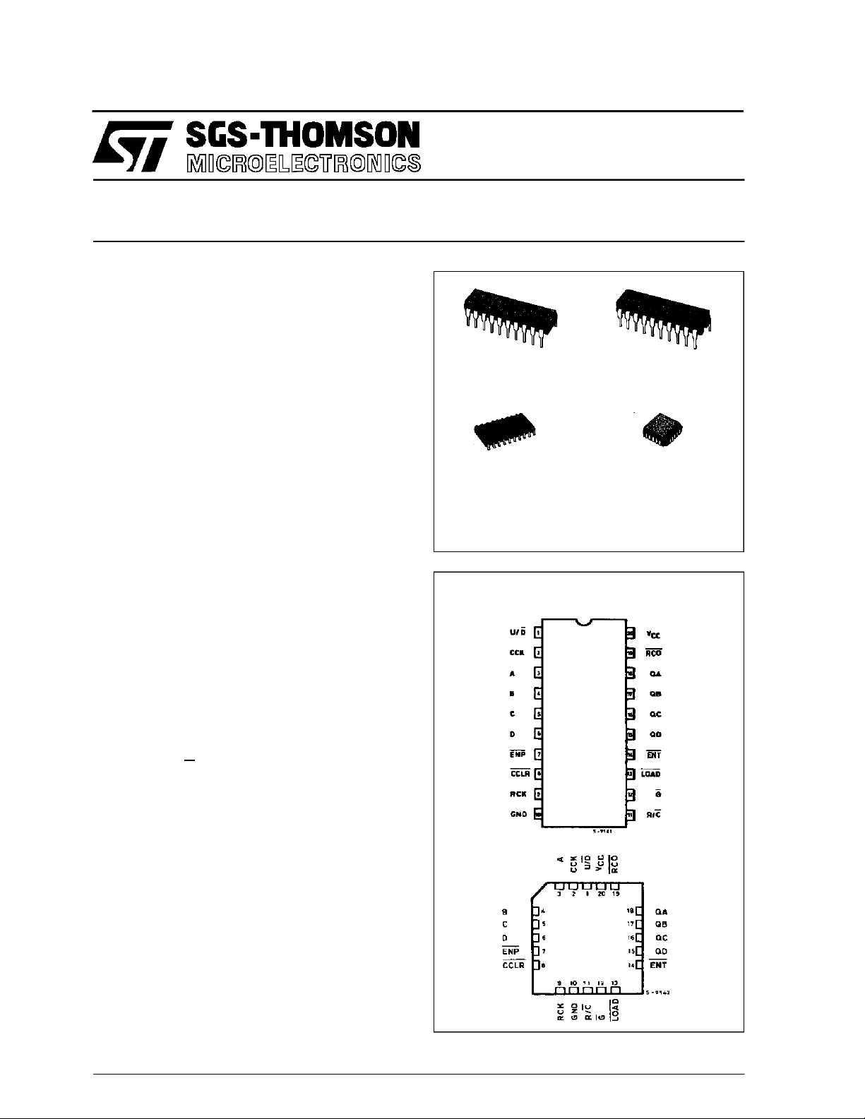
B1R
(PlasticPackage)
F1R
(CeramicPackage)
.SYMMETRICAL OUTPUT IMPEDANCE
|IOH|=IOL=6 mA (MIN.) FOR QATO Q
|IOH|=IOL=4 mA (MIN.) FOR RCO OUTPUT
.BALANCEDPROPAGATIONDELAYS
t
PLH=tPHL
.WIDE OPERATING VOLTAGERANGE
VCC(OPR)= 2 V TO6 V
.PIN AND FUNCTION COMPATIBLE
WITH LSTTL54/74LS696/697/698/699
D
M1R
(MicroPackage)
ORDER CODES :
M54HC X XXF1R M74H CXXXM1R
M74HC X XXB1R M74HCX X XC1R
C1R
(Chip Carrier)
DESCRIPTION
The HC696/697 are high speed CMOS up/down
counters fabricated with silicon gate C2MOS
technology. They achieve the highspeedoperation
similar to equivalent LSTTL while maintaining the
CMOS low power dissipation. The HC696/698 are
BCDDECADECOUNTER, andtheHC697/699 are
4-BIT BINARY COUNTER. Both devices have
register.
Theycount on the positiveedgeofthe counterclock
input(CCK) whenselected by the ”Counter Mode”.
If the input U/D is held ”H”, the internal counter
counts up, and held ”L”, counts down. The internal
counter’s outputs are stored in the output registerat
the positiveedge of registerclock (RCK).
The counter features enable P and enable T and a
ripple-carry output for easy expansion. the
register/counter select input, R/C, selects the
counter when low or the register when high for the
three state outputs, QA, QB, Qc and QD.
Boththe counterclock CCK andregister clock RCK
are positive-edge triggered. The counter clear
CCLR is active low and is synchronous for
HC698/699, and asynchronous for HC696/697.
All inputs are equipped with protection circuits
against static discharge and transient excess
voltage.
PIN CONNECTIONS (top view)
NC =
No Internal
Connection
March1993
1/22
M54/M74HC696/697/698/699
PIN DESCRIPTION
PIN No SYMBOL NAME AND FUNCTION
1 U/D Up Down Counter Selector
2 CCK Counter Clock
3, 4, 5, 6 A to D Data Inputs
7, 14 EMP/ENT Enable P and T
8 CCLR Counter Clear (Active
LOW)
9 RCK Register Clock
11 R/C Register Counter Selector
12 G Enable Input
13 LOAD Load Counter (Active
LOW)
15, 16, 17,18QA to QD Data Outputs
19 RCO Load Counter (Active
HIGH)
10 GND Ground (0V)
20 V
CC
Positive Supply Voltage
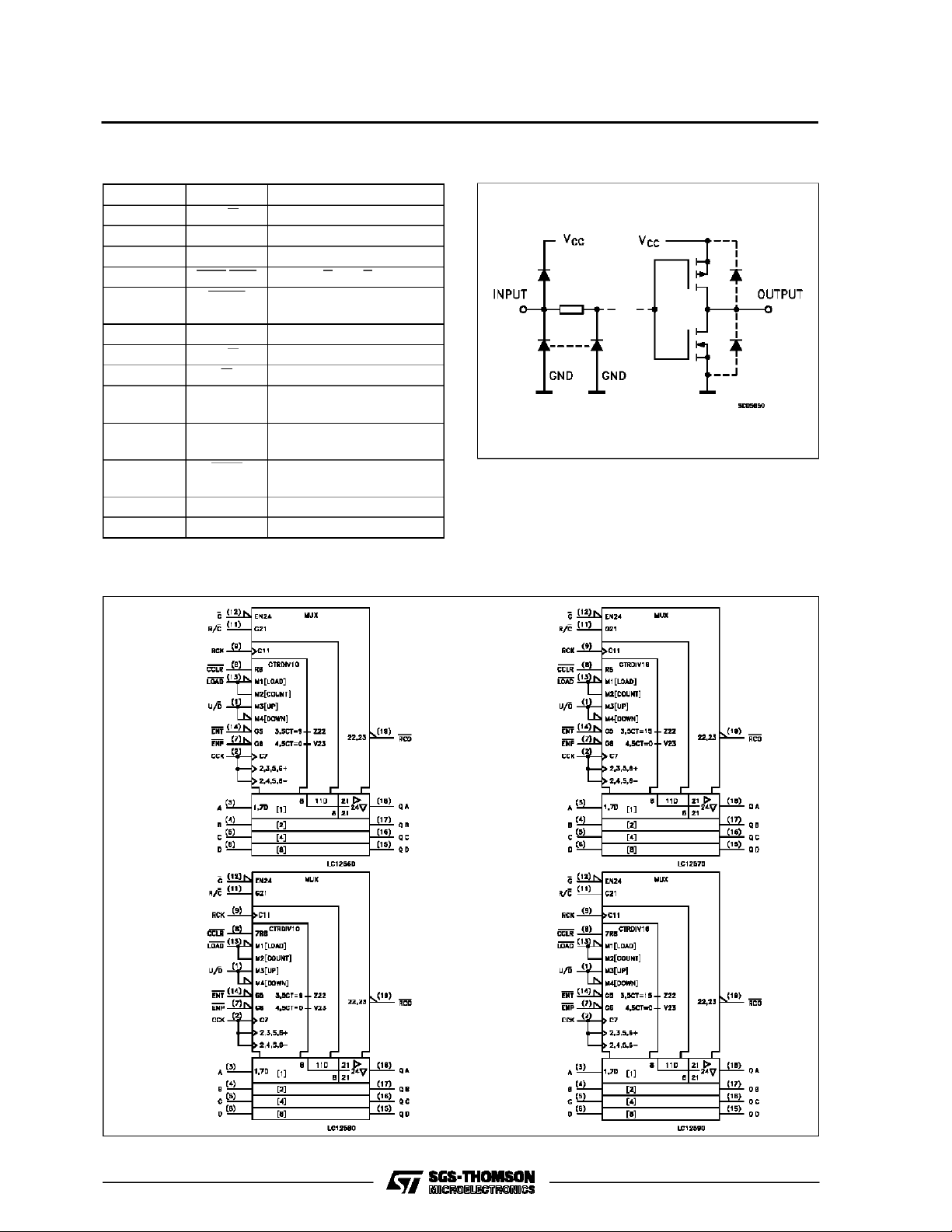
IEC LOGIC SYMBOL
INPUT AND OUTPUT EQUIVALENT CIRCUIT
HC69 6
HC69 8 HC69 9
HC69 7
2/22
TRUTH TABLE
M54/M74HC 696/697/698/699
INPUTS OUTPUTS
CCLR LOAD ENP ENT CCK U/D RCK R/C G QA QB QC QD
FUNCTION
XXXXXXXXHZZZZHIGH IMPEDANCE
L X X X X (*) X X L L L L L L CLEAR COUNTER
H L X X X X L L a b c d LOAD COUNTER
H H H X X X L L NO CHANGE NO COUNT
H H X H X X L L NO CHANGE NO COUNT
H H L L H X L L COUNT UP COUNT UP
H H L L L X L L COUNT DOWN COUNT DOWN
H X X X X X L L NO CHANGE NO COUNT
X X X X X X H L a’ b’ c’ d’ LOAD REGISTER
X X X X X X H L NO CHANGE NO LOAD
(*) : ForHC698/699
X : Don’t care
Z : Highimpedance
a-d : The levelof steady stateinputat inputs a throughD respectively
a’-d’ : The levelof steady stateoutputsat internal counter outputsQA’ throughQD’respectively
RCO function : HC696/8 - RCO= (UP• QA • QD • ENT+ UP • QA • QD • ENT)
HC697/9 - RCO = (UP • QA • QB • QC • QD • ENT + UP• QA • QB • QC • QD • ENT)
BLOCK DIAGRAM
3/22
M54/M74HC696/697/698/699
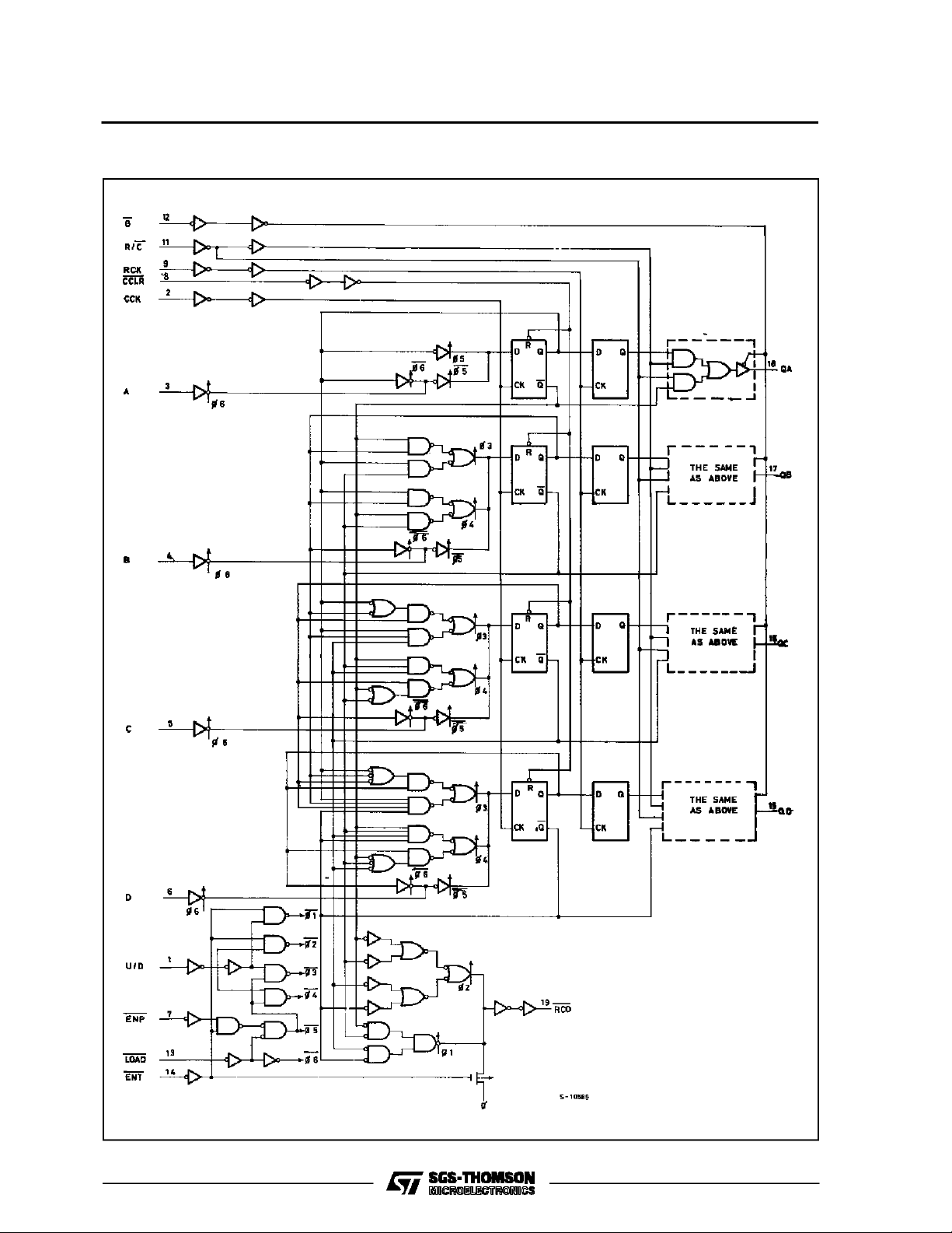
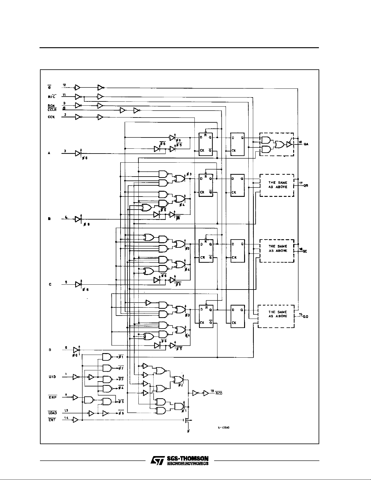
LOGIC DIAGRAM (HC696)
4/22
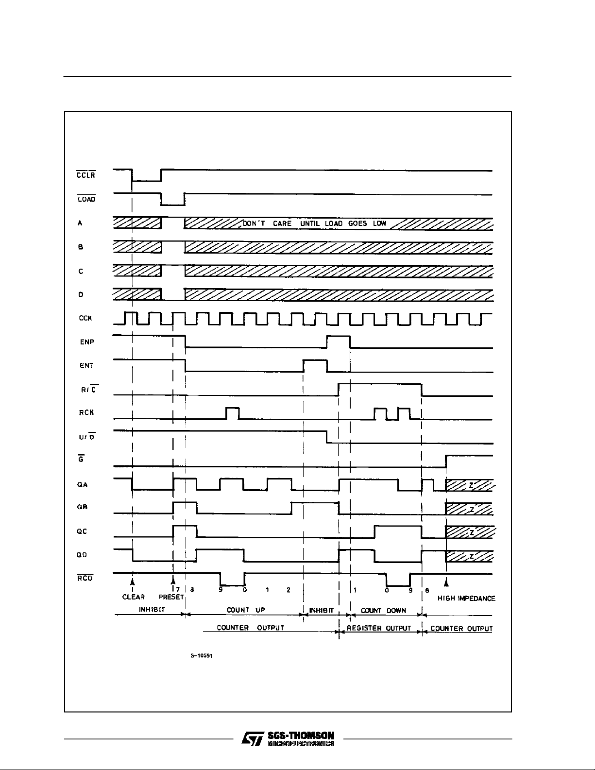
TIMING CHART (HC696)
M54/M74HC 696/697/698/699
5/22
M54/M74HC696/697/698/699
LOGIC DIAGRAM (HC697)
6/22
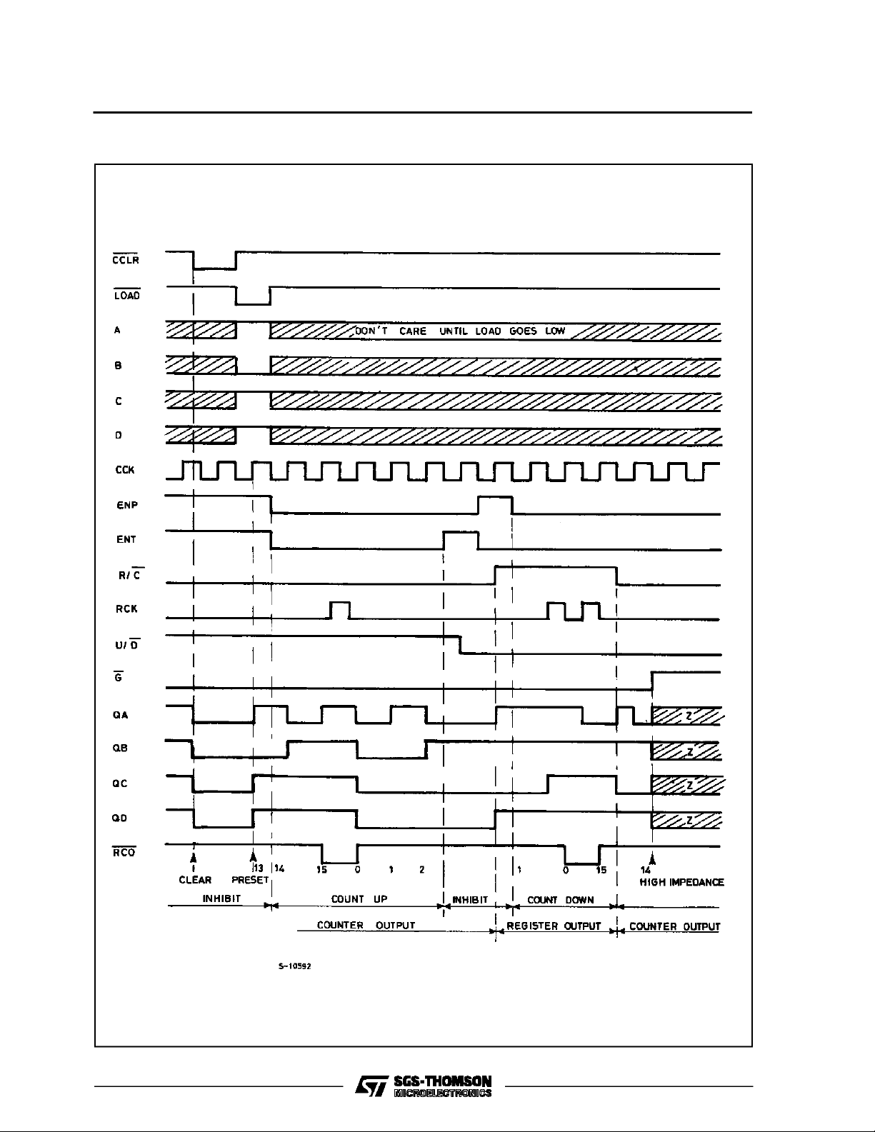
TIMING CHART (HC697)
M54/M74HC 696/697/698/699
7/22
 Loading...