

SGS Thomson Microelectronics M74HC692, M74HC691, M74HC690, M74HC693 Datasheet
M54/74HC690/691
M54/74HC692/693
HC690/692 DECADE COUNTER/REGISTER (3-STATE)
HC691/693 4 BIT BINARY COUNTER/REGISTER (3-STATE)
.HIGH SPEED
f
= 50 MHz (TYP.) at VCC=5V
MAX
.LOWPOWER DISSIPATION
ICC=4µA(MAX.) at TA=25°C
.HIGH NOISE IMMUNITY
V
NIH=VNIL
.OUTPUT DRIVE CAPABILITY
15 LSTTL LOADS (for QAto QD)
10 LSTTL LOADS (for RCO)
=28%VCC(MIN.)
B1R
(PlasticPackage)
F1R
(CeramicPackage)
.SYMMETRICAL OUTPUT IMPEDANCE
IOH =IOL= 6 mA (MIN.) (for QAtoQD)
IOH =IOL= 4 mA (MIN.) (for RCO)
.BALANCEDPROPAGATIONDELAYS
t
PLH=tPHL
.WIDE OPERATING VOLTAGERANGE
VCC(OPR)= 2 V to 6 V
.PIN AND FUNCTION COMPATIBLE
WITH LSTTL54/74LS690/691
M1R
(MicroPackage)
ORDER CODES :
M54HC X XXF1R M74H CXXXM1R
M74HC X XXB1R M74HCX X XC1R
C1R
(Chip Carrier)
DESCRIPTION
The HC690/691/692/693 are high speed CMOS
COUNTER/REGISTER fabricated in silicon gate
C2MOS technology.
They have the same high speed performance of
LSTTL combined with true CMOS low power consumption.
The internal circuitis composedof 3 stages including buffer output, which offers high noise immunity
andstableoutput.Thesedevices incorporateasynchronous counter, four-bit D-type register, and
quadruple two-line to one-line multiplexers with
three-state outputs in a single 20-pin package. The
counter can be programmed from the data inputs
andhaveenableP andenable Tinputsand a ripplecarry output for easy expansion. The register/counter select input, R/C, selects the counter
when low or the register when high for the threestateoutputs, QA, QB, QC, and QD.
If the LOADinput (LOAD)is held ”L” DATAinput(AD) are loaded in to the internal counter at positive
edge of counter clock input (CCK). In the counter
mode, internal counter counts up at the positive of
the counter clock.If thecounter clear input (CCLR)
isheld”L”, theinternal counteriscleared(synchronously to the counter clock for HC692/HC693, and
asynchronously for HC690/HC691). The internal
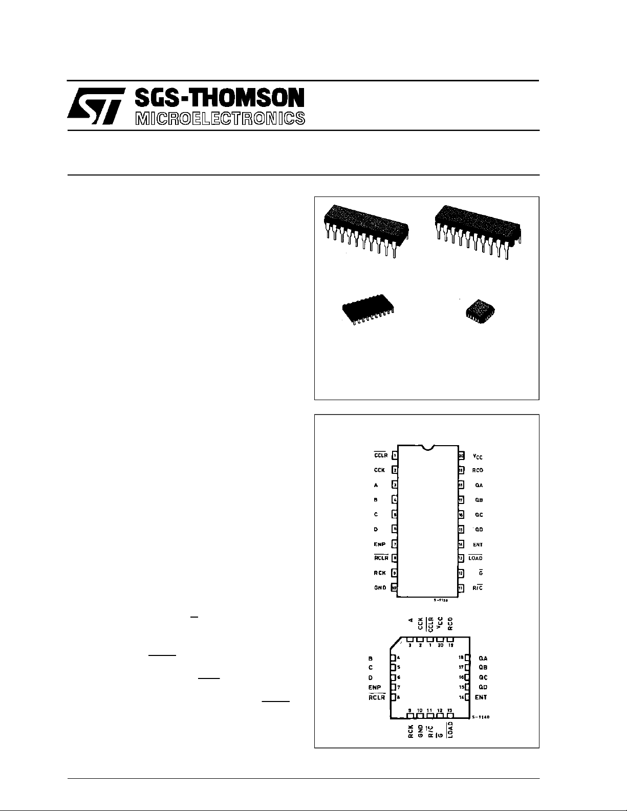
PIN CONNECTIONS (top view)
NC =
No Internal
Connection
March1993
1/23
M54/M74HC690/691/692/693
counter’s outputs are stored in the output registerat
the positiveedge of the register clock (RCK). If the
register clear input(RCLR) is held ”L” the registeris
cleared (synchronously to register clock for
HC692/HC693 and asynchronously for
HC690/HC691).Allinputsare equipped withprotection circuits against static discharge and transient
excessvoltage.
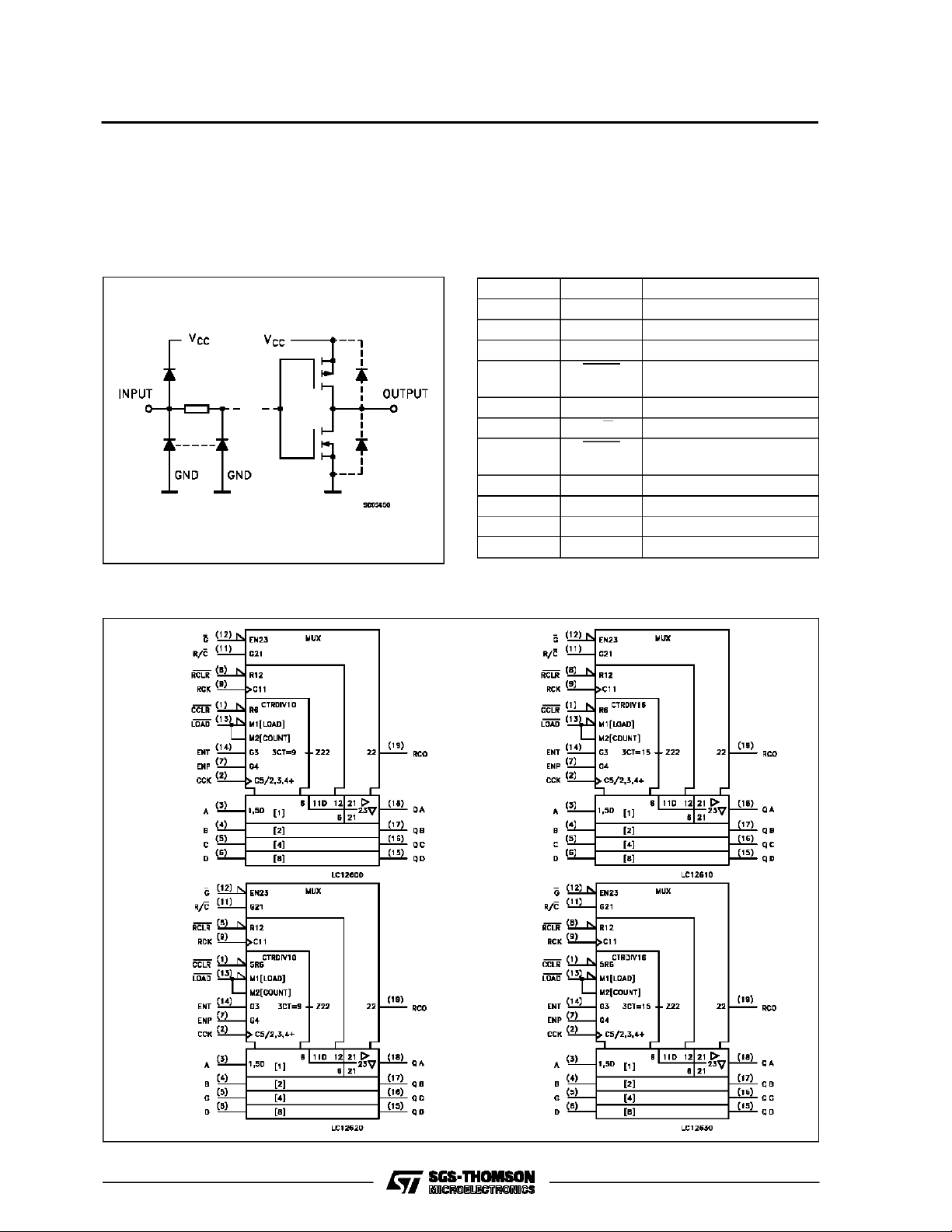
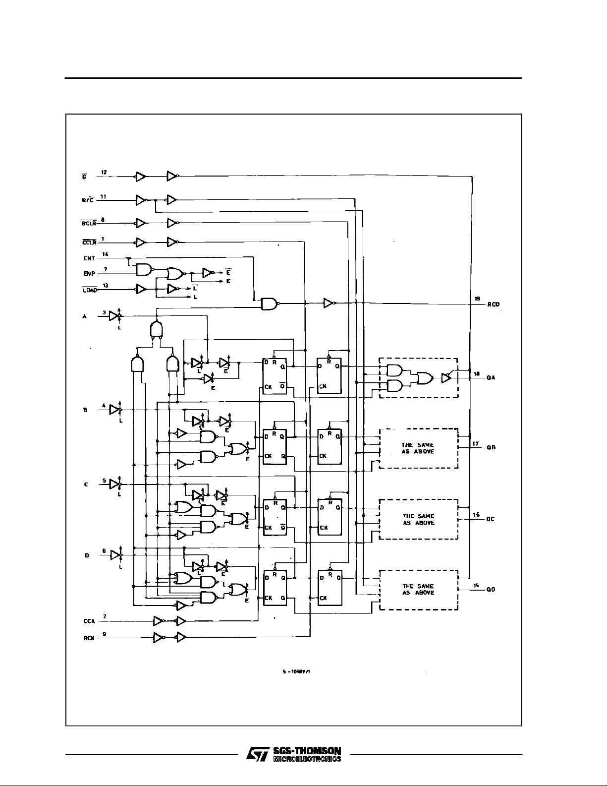
INPUT AND OUTPUT EQUIVALENT CIRCUIT PIN DESCRIPTION
PIN No SYMBOL NAME AND FUNCTION
3 to 6 A to D Data Inputs
7, 14 ENT, ENP Enable Inputs
15 to 18 QA to QD Data Outputs
1 CCLR Counter Clear (Active
2 CCK Counter Clock
11 R/C Counter/ Register Select
8 RCLR Register Clear (Active
9 RCK Register Clock
19 RCO Ripple Counter Output
10 GND Ground (0V)
20 V
CC
IEC LOGIC SYMBOLS
LOW)
LOW)
Positive Supply Voltage
HC69 0
HC69 2 HC69 3
HC69 1
2/23
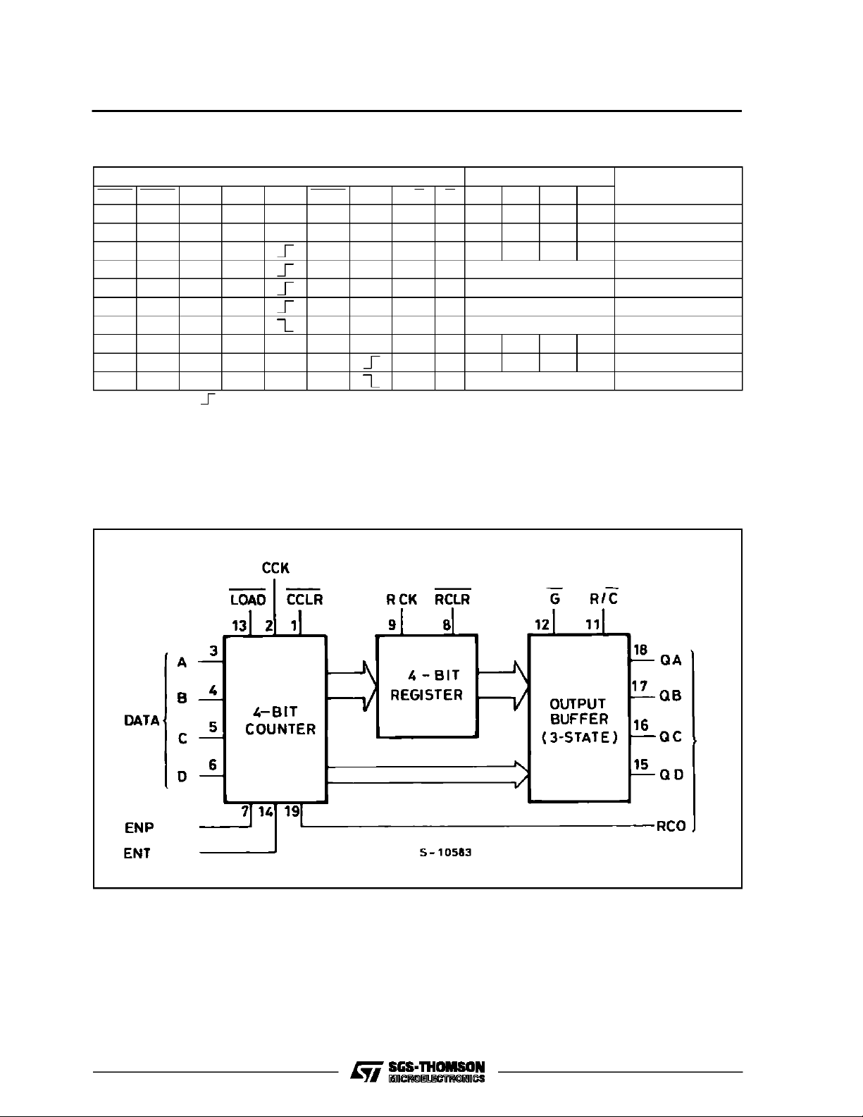
TRUTH TABLE
M54/M74HC 690/691/692/693
INPUTS OUTPUS
CCLR LOAD ENP ENT CCK RCLR RCK R/C G QA QB QC QD
FUNCTION
XXXXXXXXXZZZZHIGH IMPEDANCE
L X X X (*) X X L L L L L L CLEAR COUNTER
H L X X X X L L a b c d LOAD COUNTER
H H L X X X L L NO CHANGE NO COUNT
H H X L X X L L NO CHANGE NO COUNT
H H H H X X L L COUNT UP COUNT UP
H X X X X X L L NO CHANGE NO COUNT
X X X X X L (*) H L L L L L CLEAR REGISTER
X X X X X H H L a’ b’ c’ d’ LOAD REGISTER
X X X X X H H L NO CHANGE NO LOAD
(*): X for HC690/691
X : DON’T CARE
Z : HIGH IMPEDANCE
a-d :THE LEVELOF STEADY STATEINPUTSAT INPUTS ATHROUGHTD RESPECTIVELY.
a’-d’ : THELEVEL OF STEADYSTATE OUTPUTSAT INTERNALCOUNTEROUTPUTSa’ through qd’ respectively
HC690/692 RCO = QA• QD • ENT
HC691/693 RCO = QA• QB • QC • QD • ENT
forHC692/693
BLOCK DIAGRAM
3/23
M54/M74HC690/691/692/693
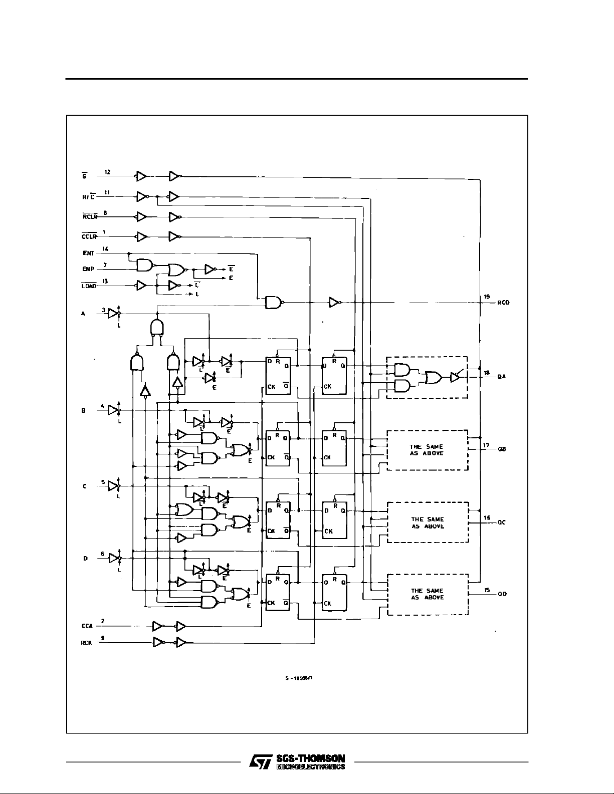
LOGIC DIAGRAM (HC690)
4/23
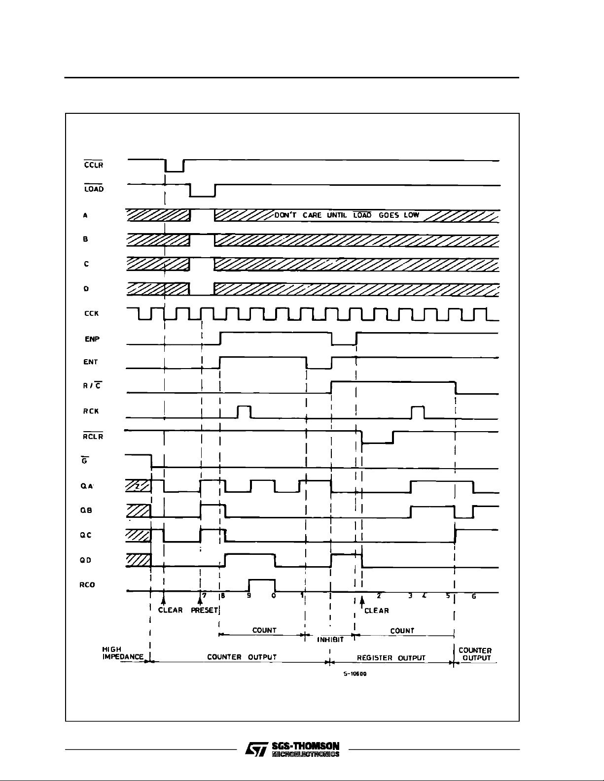
TIMING CHART (HC690)
M54/M74HC 690/691/692/693
5/23
M54/M74HC690/691/692/693
LOGIC DIAGRAM (HC691)
6/23

TIMING CHART (HC691)
M54/M74HC 690/691/692/693
7/23
 Loading...