

SGS Thomson Microelectronics M74HC652, M74HC651 Datasheet
M74HC651
M74HC652
HC651 OCTAL BUS TRANSCEIVE R/REGISTER (3-STATE, INV.)
HC6 52 OCTAL BUS TRANSCE IVER/REG ISTER (3-STATE)
. HIGH SPEED
f
= 73 MHz (TYP.)AT VCC=5V
MAX
.LOWPOWERDISSIPATION
ICC=4µA(MAX.) AT TA=25°C
.HIGH NOISEIMMUNITY
V
NIH=VNIL
=28%V
CC (
MIN.)
.OUTPUT DRIVE CAPABILITY
15 LSTTL LOADS
.SYMMETRICALOUTPUT IMPEDANCE
IOH =IOL= 6 mA(mIN.)
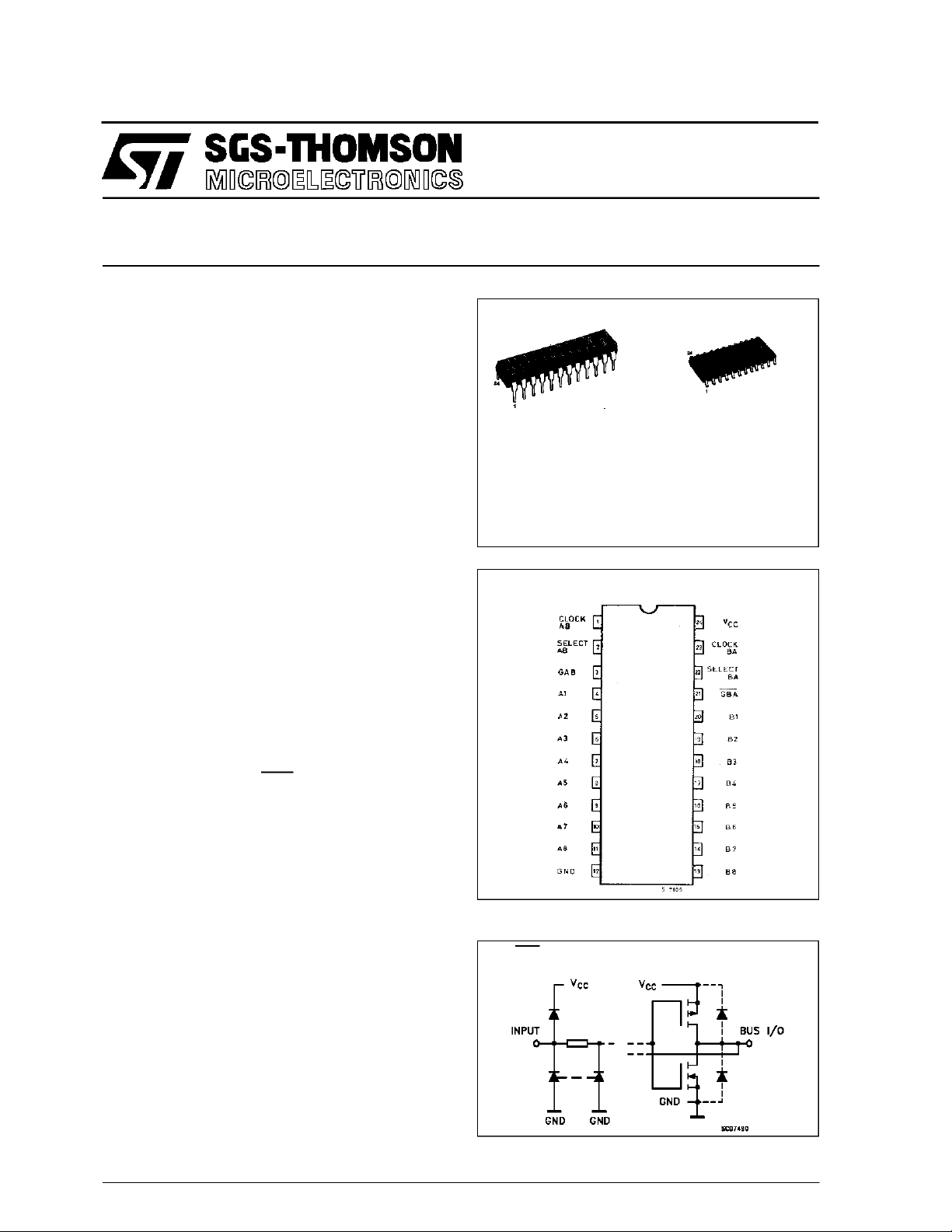
B1R
(PlasticPackage)
M1R
(MicroPackage)
.BALANCEDPROPAGATION DELAYS
t
PLH=tPHL
.WIDE OPERATINGVOLTAGE RANGE
VCC(OPR)= 2 VTO 6V
M74HC X XXM1R M74HC XXXB1R
ORDER CODES :
.PIN ANDFUNCTION COMPATIBLE
WITH 54/74LS651/652
DESCRIPTION
M74HC651/652 are high speed CMOS OCTAL
BUS TRANSCEIVERS AND REGISTERS (3STATE), fabricated in silicongate C2MOS technology. They have the same high speedperformance
ofLSTTLcombined withtrueCMOS low powerconsumption.These devices consist of bustransceiver
circuits, D-type flip-flops, and control circuitry arrangedfor multiplexed transmission ofdatadirectly
from the input bus or fromthe internal storage registers.EnableGABand GBAare provided tocontrol
the transceiver functions.
SelectAB and Select BA control pins are provided
to select whether real-time or stored data is transfered. A low input level selects real-time data, and
a high selects stored data.
Data onthe Aor B bus, or both,can be storedin the
internal D flip-flops by low-to-high transitions at the
appropriate clock pins (CLOCK AB or CLOCK BA)
regardless oftheselectorenablecontrolpins.When
selectAB andselectBA arein thereal-time transfer
mode,it isalso possible to store datawithout using
the internal D-type flip-flops by simultaneously enablingGABandGBA. Inthisconfiguration eachoutput reinforces its input. Thus, when all other data
sources to the two setsof bus lines are at high impedance,each set of buslines will remain at its last
state.Allinputsare equipped withprotectioncircuits
against static discharge and transient excess voltage.
INPUT AND OUTPUT EQUIVALENT CIRCUIT
PIN CONNECTIONS (top view)
GAB,GAB,CAB, A, B
SAB,SBA, CBA
October 1993
1/12
M74HC651/652
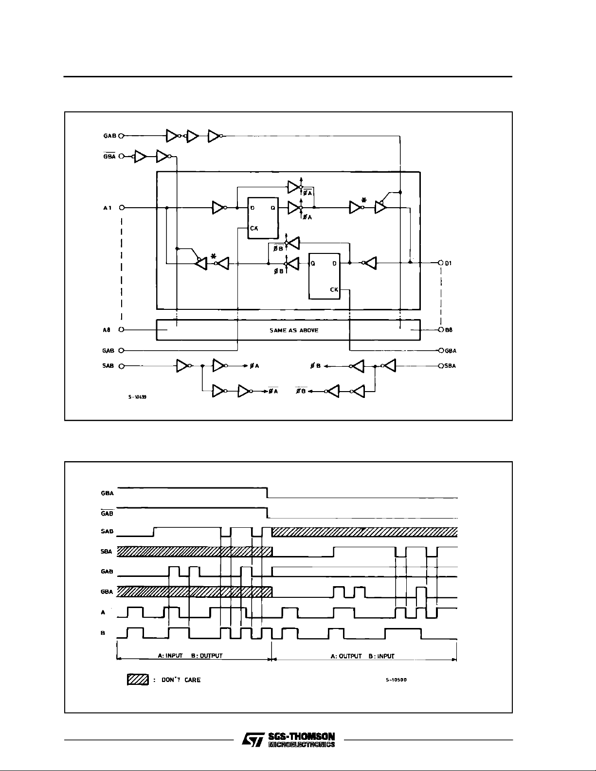
LOGIC DIAGRAM (HC652)
Note: In case ofM74HC652 output invertermarked * atA bus and B busare eliminated.
TIMING CHART
2/12
M74HC651/652
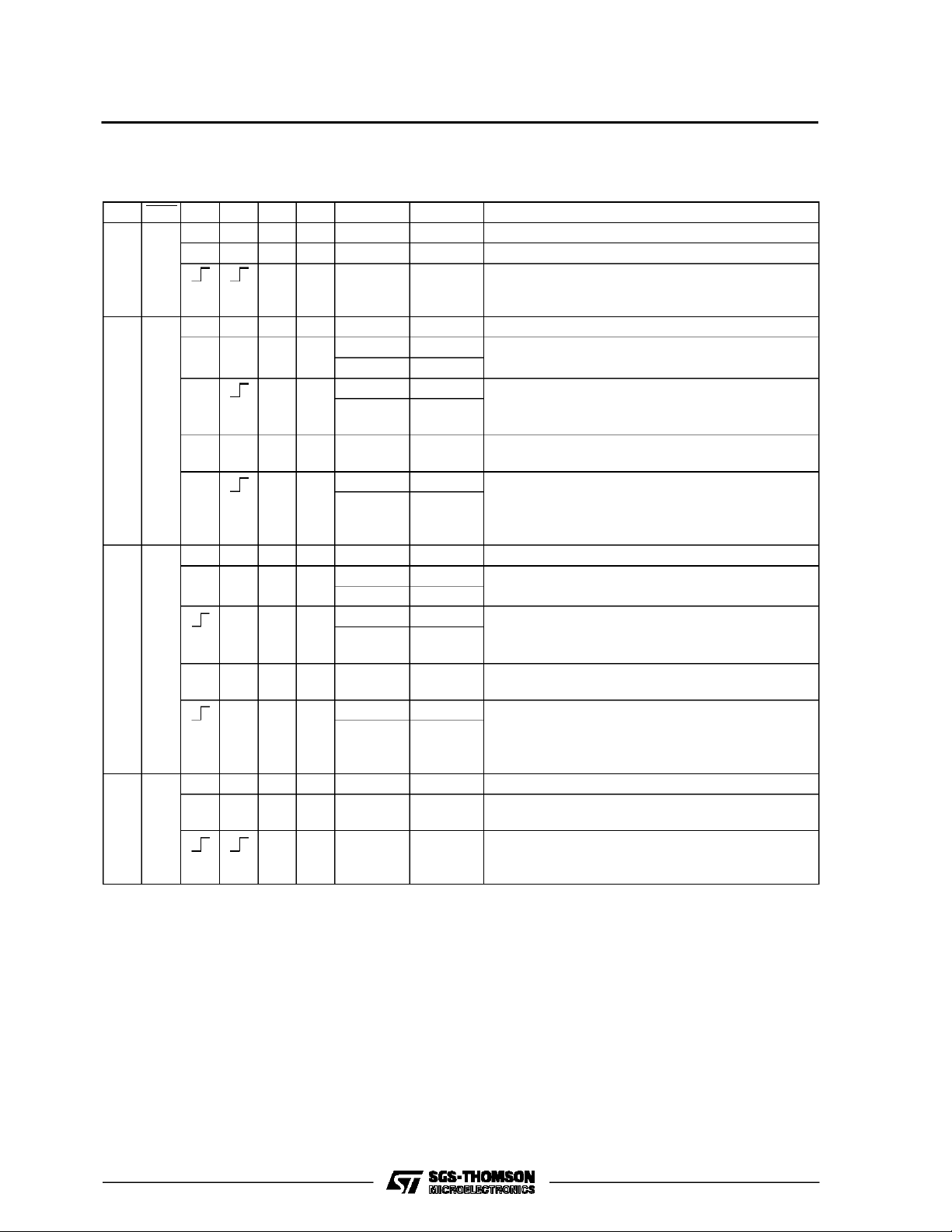
TRUTH TABLE
HC652 ( The truth table for HC651 is t he same as this, but with the outputs inverted)
GAB GBA CAB CBA SAB SBA A B FUNCTION
INPUTS INPUTS Both the A bus and the B bus are inputs
LH
LL
HH
HL
X : DON’TCARE
Z :HIGH IMPEDANCE
Qn :THE DATA STOREDTO THEINTERNALFLIP-FLOPSBY MOST RECENTLOWTO HIGHTRANSITION OF THECLOCK INPUTS
* : THEDATA AT THE A ANDB BUSWILLBE STORED TO THE INTERNALFLIP-FLOPS ON EVERY LOWTO HIGH TRANSITIONOF
THECLOCK INPUTS
X X X X Z Z The output functions of the A and B bus are disabled
X X INPUTS INPUTS Both the A and B buz are used for inputs to the
internal flip-flops. Data at the bus will be stored on
low to high transition of the clock inputs
OUTPUTS INPUTS The A bus are outputs and the B bus are inputs
X* X X L L L The data at the B bus are displayed at the A bus
HH
X* X L L L The data at the B bus ar displayed at the A bus.
HH
The data of the B bus are stored to the internal
flip-flop on low tohigh transition of th clock pulse
X* X X H Qn X The data stored to the internal flip-flop are dispayed
at the A bus
X* X H L L The data at the B bus are stored to the internal flip-
HH
flop on low to high transition of the clock pulse. The
states of the internal flip-flops output directly to the
A bus
INPUTS OUTPUTS The A bus are inputs and the B bus are outputs
XX*L X
L L The data at the A bus are displayed at the B bus
HH
X* L X L L The data at the A bus are displayed at the B bus.
HH
The data of the A bus are stored to the internal flipflop on low to high transition of the clock pulse
X X* H X X Qn The data stored to the internal flip-flops are
displayed at the B bus
X* H X L L the data at the A bus are stored to the internalflip-
HH
flop on low to high transition of the clock pulse. The
states of the internal flip-flops output directly to the
B bus
OUTPUTS OUTPUTS Both the A bus and the B bus are outputs
X X H H Qn Qn The data stored to the internal flip-flops are
displayed at the A and B bus respectively
H H Qn Qn The output at the A bus are displayed at the B bus,
the output at the B bus are displayed at the A bus
respectively
3/12
M74HC651/652
PIN DESCRIPTION
PIN No SYMBOL NAME AND FUNCTION
1 CLOCK AB A to B Clock Input (LOW to HIGH, Edge-Trigged)
2 SELECT AB Select A to B Source Input
3 GAB Direction Control Input
4, 5, 6, 7, 8, 9, 10, 11 A1 to A8 A data Inputs/Outputs
20, 19, 18, 17, 16, 15, 14, 13 B1 to B8 B Data Inputs/Outputs
21 GBA Output Enable Input (Active LOW)
22 SELECT BA Select B to A Source Input
23 CLOCK BA B to A Clock Input (LOW to HIGH, Edge-Triggered)
12 GND Ground (0V)
24 V
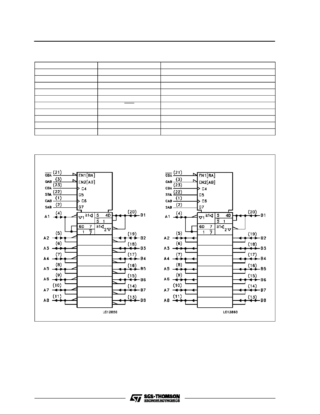
IEC LOGIC SYMBOLS
CC
HC651 HC652
Positive Supply Voltage
4/12
 Loading...